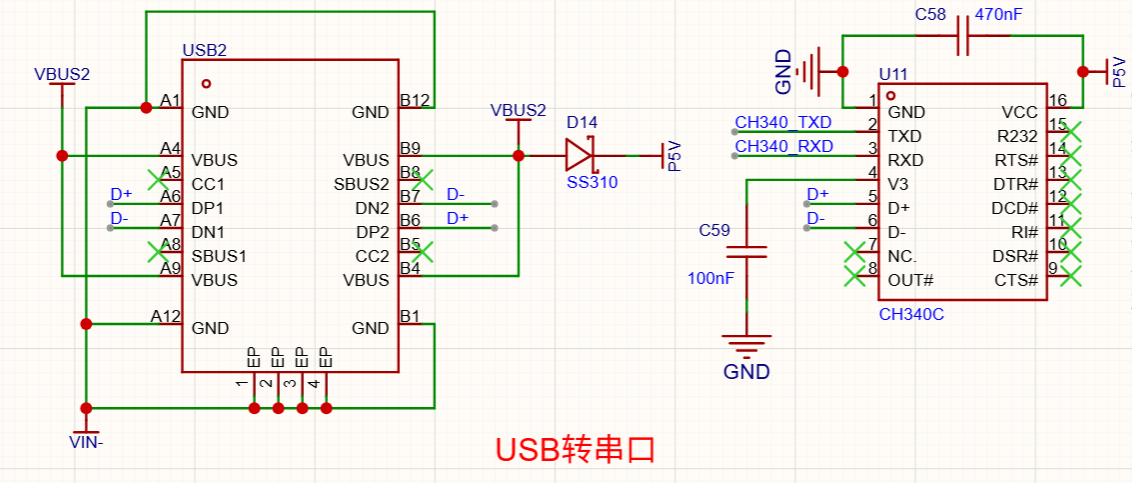
Connecting VIN- allows the input current to pass through the sense resistor, so that the input current can still be sensed even if only USB2 is connected.
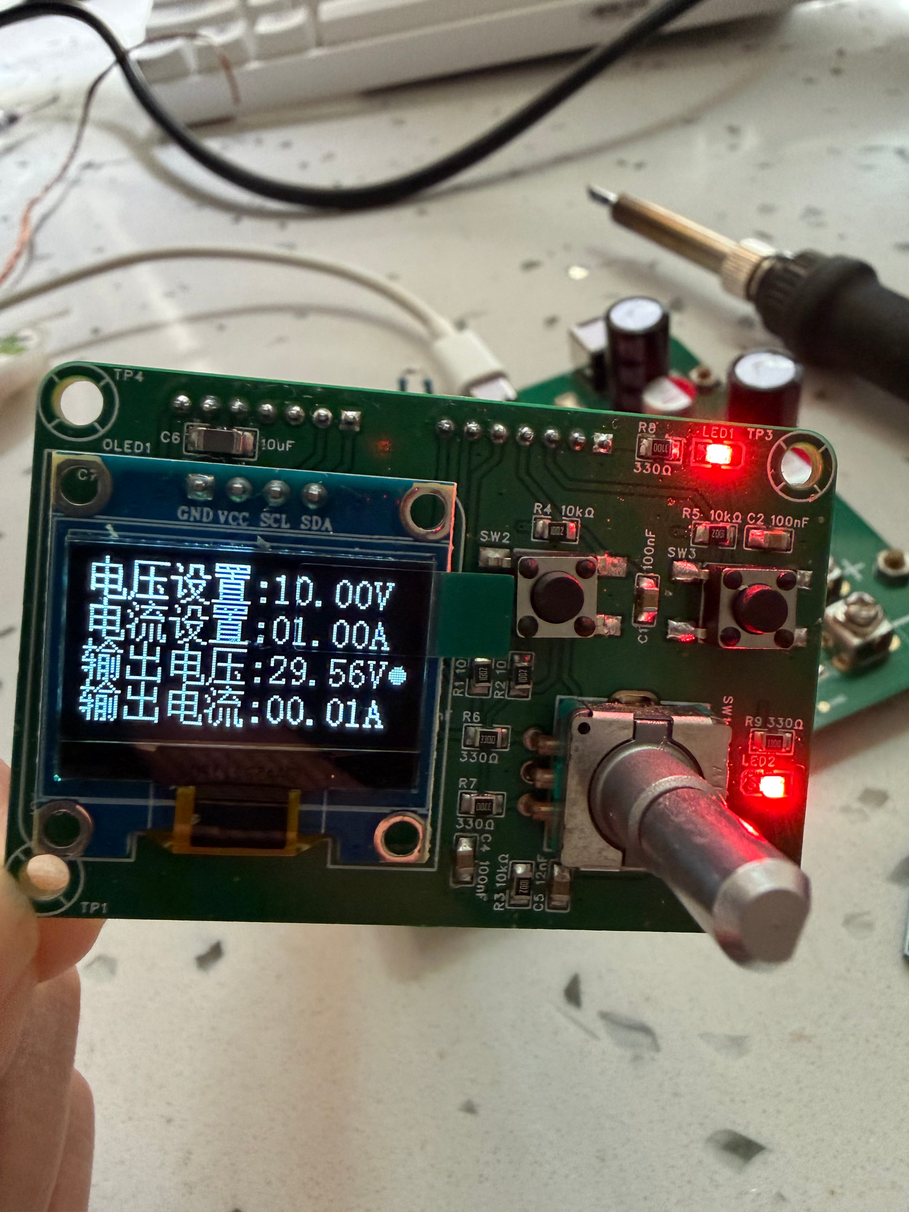
Hey, have you ever used HRTIM fault events when writing your software? I’m using a comparator to directly shut off the MOSFET via hardware when the inductor current exceeds my setpoint. However, during the soft start, I noticed that my PWM output seems to be disabled. I suspect the capacitor charging current is too high, which causes it to hit my setpoint and disable the PWM output. I want to know how to configure the STM32’s HRTIM to implement Cycle-by-Cycle—meaning that during soft start, if the inductor current hits my set maximum limit, the PWM output shuts off immediately but automatically turns back on in the next cycle.
Have you calibrated your measurement circuit? The circuit board you designed will have many parasitic parameters, causing slight variations in the measurement circuit’s gain. It needs to be calibrated before it can accurately output the correct values.
Has the software been modified? Check if there are any issues with the sampling circuit.
Guru, I’ve added hardware overcurrent protection (cycle-by-cycle current limiting) and slowed down the open-loop soft start (now 500Hz, step size 0.001). I didn’t add a current inner loop because I figured I should get the open-loop done first before adding closed-loop.
-
When testing on the board, I found that the circuit works normally under no load. But after I added a 20R load (with output voltage Vo set to 30V), the MOSFET failed again. What could be the reason for this?
-
The circuit and code are exactly the same for no-load and loaded conditions, so why does the MOSFET get damaged?
-
What should be my next step? Should I reduce the output capacitance? Because previously, when my output capacitance was relatively small, the circuit could work normally under load. But after I increased the output capacitance and powered it on, the MOSFET blew. If I reduce the output capacitance, will the circuit work normally again? Why does this happen?
This is a very typical issue; the inrush current charging the output capacitors during soft-start can easily cause a false over-current protection trigger. If you’re using HRTIM Fault Latched mode, once triggered, it will remain shut off until manually cleared by software, which explains the „PWM completely disabled
Your problem is very typical: surviving at no-load but blowing up under load. This shows your open-loop soft start completely failed the “current stress” test.
To directly answer your three questions first:
-
It works at no-load but blows up with a 20Ω load because, during loaded startup, the inductor current = output capacitor charging current + load current. At no-load, the inductor only charges the capacitor, so the current is small; with a 20Ω load (1.5A), under the same duty cycle stepping, the inductor has to bear this extra 1.5A DC component, and the peak current easily punches right through your inductor’s 12A saturation point. Once the inductor saturates, it’s equivalent to a piece of wire, and 58V is directly slammed across the MOSFET’s Rds(on) and trace resistance, resulting in tens of amps instantly. Your “cycle-by-cycle current limiting” either has the wrong sampling point, or its response speed can’t keep up with the current rise slope after saturation, so it provides no real protection.
-
The code is the same, but the operating conditions are worlds apart. Open-loop control is blind; it doesn’t care if the output is no-load or full-load, it just pushes the duty cycle with fixed steps. No-load startup is a “stroll in the park,” while loaded startup is “climbing a mountain with a heavy pack.” If you make the circuit run at the same pace, the peak inductor current under load could be several times that of no-load. It’d be weird if it didn’t blow up.
-
Reducing the output capacitor indeed prevents blowing it up temporarily, because the charging charge required at the startup instant is reduced, the peak inductor current drops, and it stays further from the saturation point. But this is just hiding your head in the sand—you can’t seriously only use small capacitors in your final product, can you? The root cause is that your control lacks current limiting. The next thing you should do isn’t tweaking the capacitor, but immediately putting a sense resistor (or current probe) in series with the inductor loop and using an oscilloscope to capture the current waveform during loaded startup to see exactly how high the peak goes.
Specific Analysis and Recommendations:
Right now, you’re basically “running half-naked”—you have hardware OCP but no current closed-loop. A soft start step of 0.001 sounds gentle, but when starting up with a large capacitor + load, the peak inductor current has long exceeded 12A. Although the CSD19534Q5A can handle a pulsed current of 100A, that’s premised on the inductor not saturating and the current being controlled. Once the inductor saturates, the current is uncontrolled, and the silicon die in the FET melts through in microseconds, shorting G, D, and S entirely.
Why does only the Buck side blow up?
In Buck mode, the Buck high-side switch is the main switch, directly facing the 58V input and the “near short-circuit” of the saturated inductor. The Boost high-side switch is normally on, only passing the relatively smooth load current, without the double whammy of high-frequency hard-switching + saturation surge that the Buck high-side switch experiences. Energy comes from the input, and the Buck high-side switch is the first gate; it dying first is completely normal.
What you should do next (by priority):
-
Capture the waveform to confirm the cause of death: Reduce the output capacitor back to 470uF, attach a 20Ω load, series a 0.1Ω sense resistor with the inductor (or use a current probe directly), and look at the startup current with an oscilloscope. I bet your startup peak exceeds 15A. If reducing the capacitor drops the peak to under 10A and it starts normally, it confirms that startup current saturation caused the blown FET.
-
Check your hardware OCP: Where is the sampling point for the cycle-by-cycle current limiting? If it’s sampling the Buck low-side switch (freewheeling period) current, then you can’t see the current spike at all during the high-side switch’s on-time; there’s a blind spot of at least 1 switching cycle. Inductor saturation often occurs during the high-side on-time; by the time you detect overcurrent during the low-side on-time, the high-side switch has already turned to slag. Recommendations:
- Set the current limit to 8~9A (leave a margin of over 3A, don’t set it right against 12A)
- Ensure the total delay from overcurrent detection to PWM shutdown is <500ns
- If using low-side sampling, consider switching to bus or inductor high-side sampling, or at least add a comparator for hardware fast shutdown
-
Stop stubbornly sticking with open-loop: You’ve proven twice that open-loop loaded startup isn’t viable. Hurry up and add an inner current loop, even if it’s the most basic peak current limit—add a limiter after the voltage loop output to clamp the current reference within 10A; if exceeded, directly kill the PWM. This works better than any soft start step. Dual closed-loop (outer voltage loop + inner current loop) is the bare minimum for a Buck-Boost; it’s not optional.
-
The inductor is already dead: You mentioned the inductor has burn marks, so this inductor is no longer reliable. Once a Sendust core goes into deep saturation, its permeability permanently drops, and it might saturate at 8A next time. It’s recommended to replace it with an inductor with a saturation current of 20A or more, or at least a brand new one of the same model. Don’t skimp on this; blowing up another MOSFET is more expensive.
-
Output capacitance can be increased, but startup must be current-limited: Large capacitors are fine, but you must use constant current charging during startup. Mature solutions limit the inductor current first (e.g., 5A), and switch to a constant voltage closed-loop once the output voltage climbs near the target value. Your current open-loop soft start is essentially “blindly bumping around with a constant duty cycle”—if you bump right, it lives; if you bump too hard, it blows.
Summary: Reducing the output capacitor lets you temporarily run experiments, but as long as you’re still doing open-loop + heavy load startup, blowing the FET is just a matter of time. The top priority is to capture the current waveform to confirm the saturation point, and then implement an inner current loop. Stop obsessing over the capacitance value; that’s just a symptom. The missing control loop is the root cause.
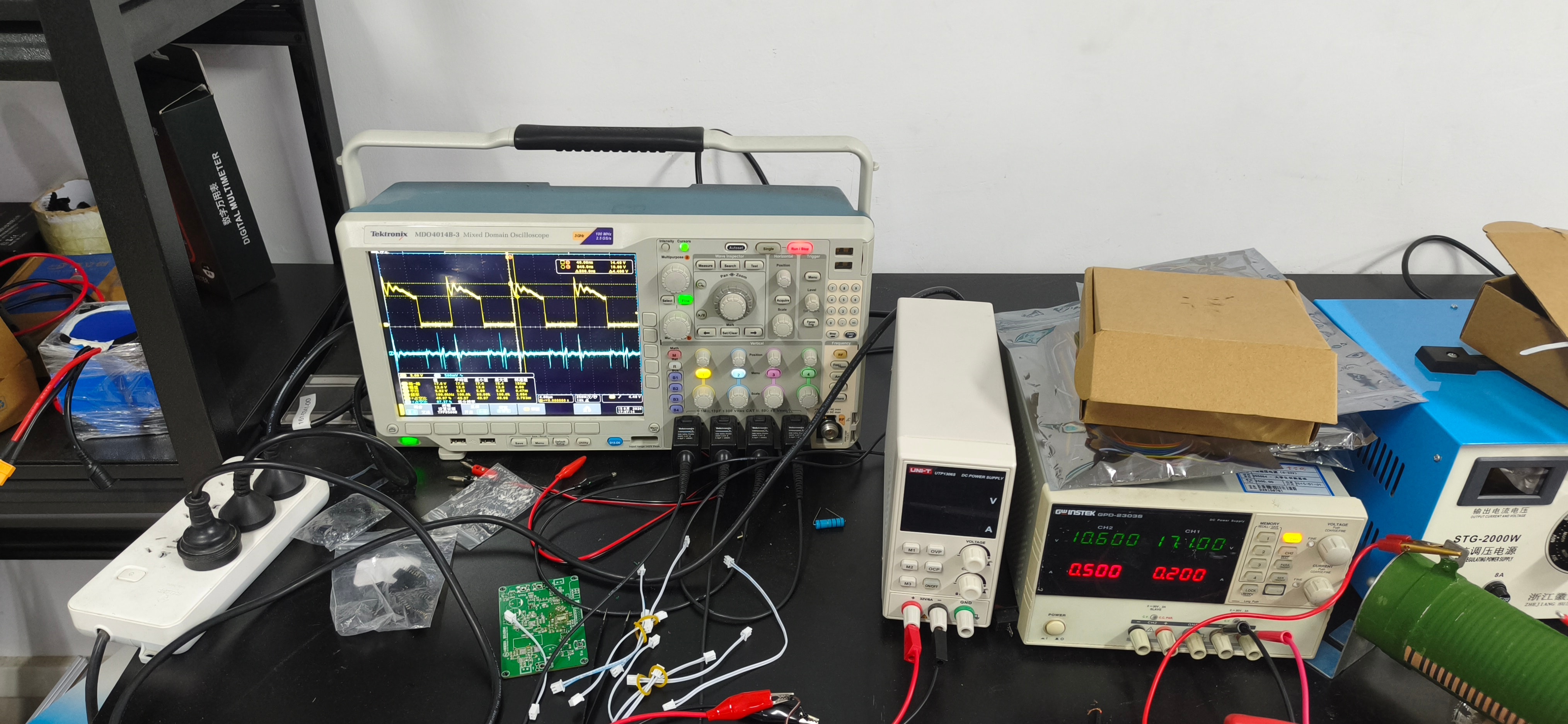
I laid out a new version, but the SW pin on the buck side ended up like this (yellow line). I also tested my high-side switch drive waveform (red line). What should I modify? The bootstrap capacitor? Or something else? I didn’t have this issue in my previous revisions; what is causing this problem?
-
My test was at 17V and 0.2A input, running at a fixed duty cycle of 0.5 with no load (a 10K resistor, makes no difference whether it’s added or not), and the output was around 6.5V (I did the math, and based on the inductor voltage balance, it is indeed this value). I don’t understand why the SW node voltage is a trapezoidal wave like this.
-
The yellow line in the first image is the inductor current waveform.
-
This image looked quite clear on my phone, so I’m not sure why it became blurry after uploading.
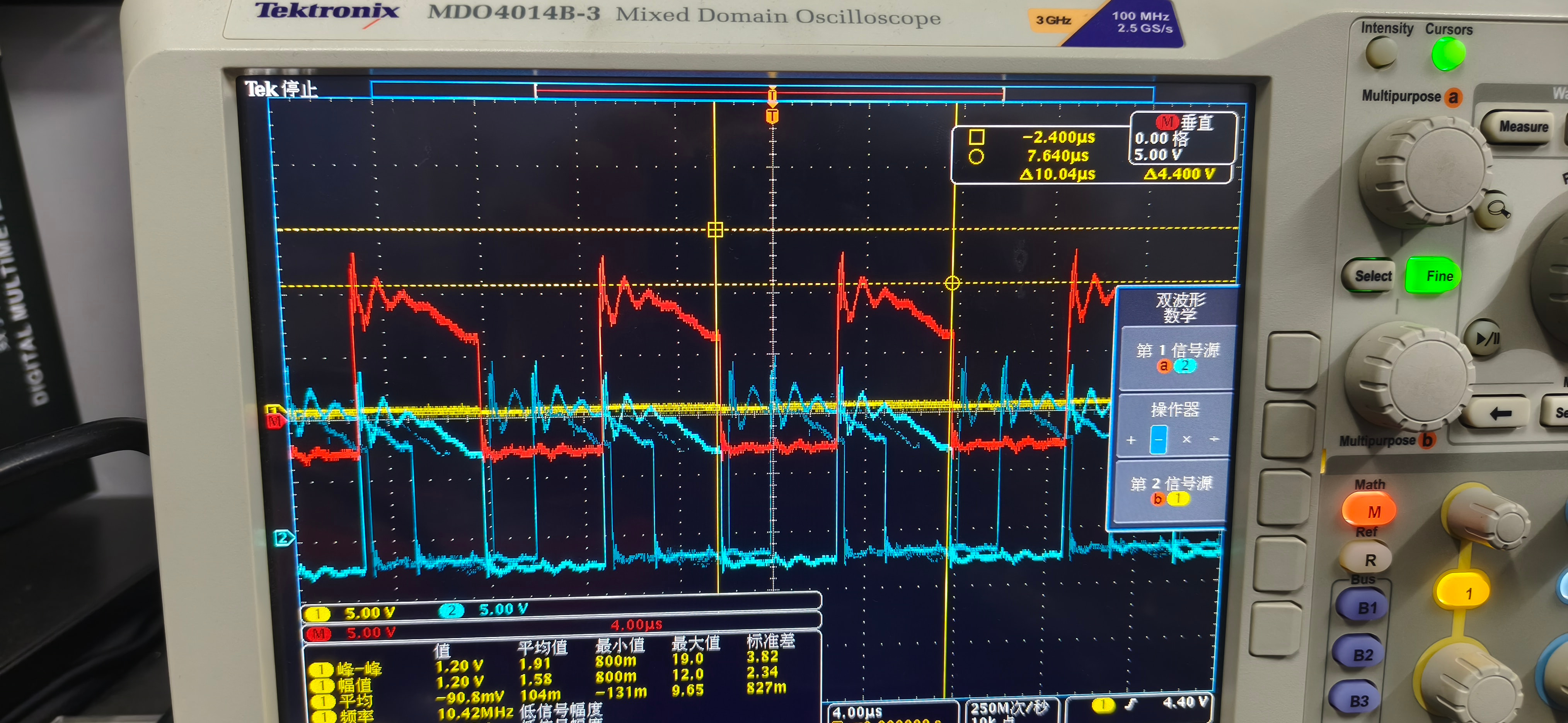
What was changed?
Take a look at the layout
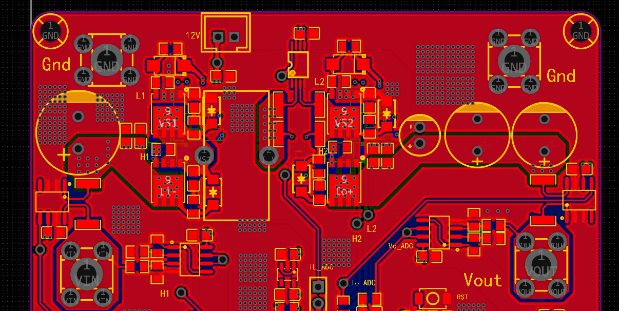
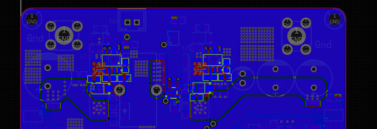
On the back is the MOS driver. I changed the resistor to 8R, but the symptom remains the same (previously I was using 4R).
The RC and diode in parallel with the MOSFET are not soldered.
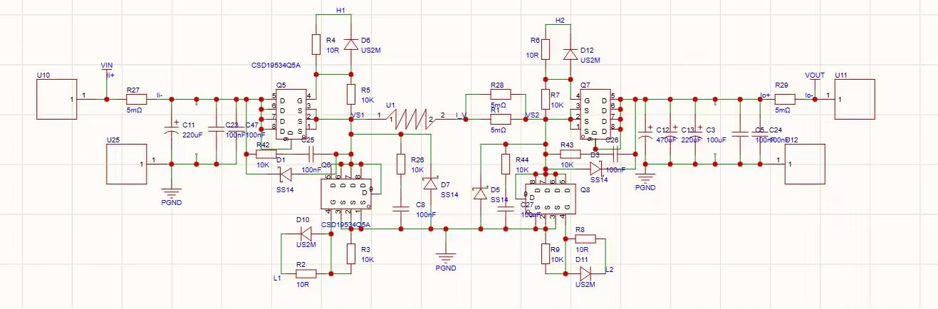
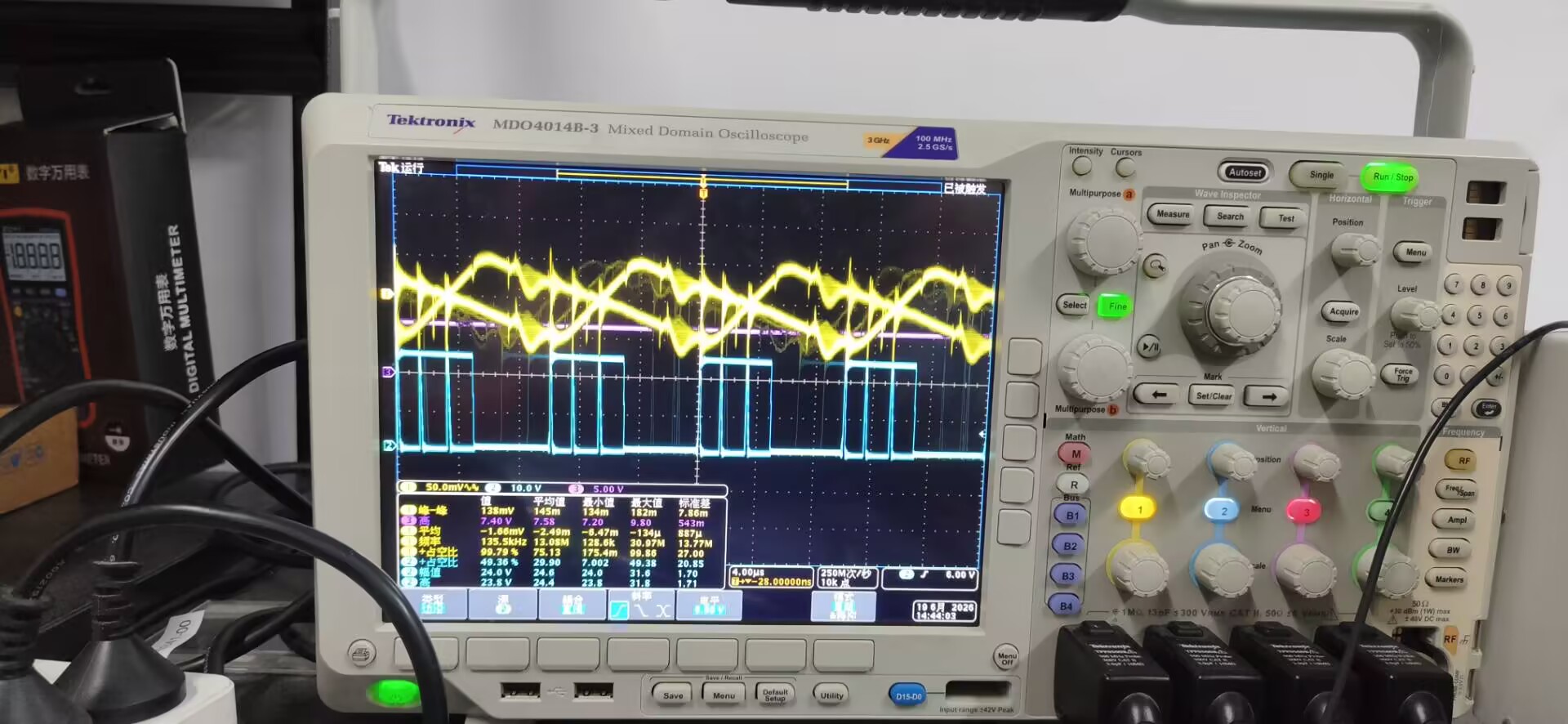
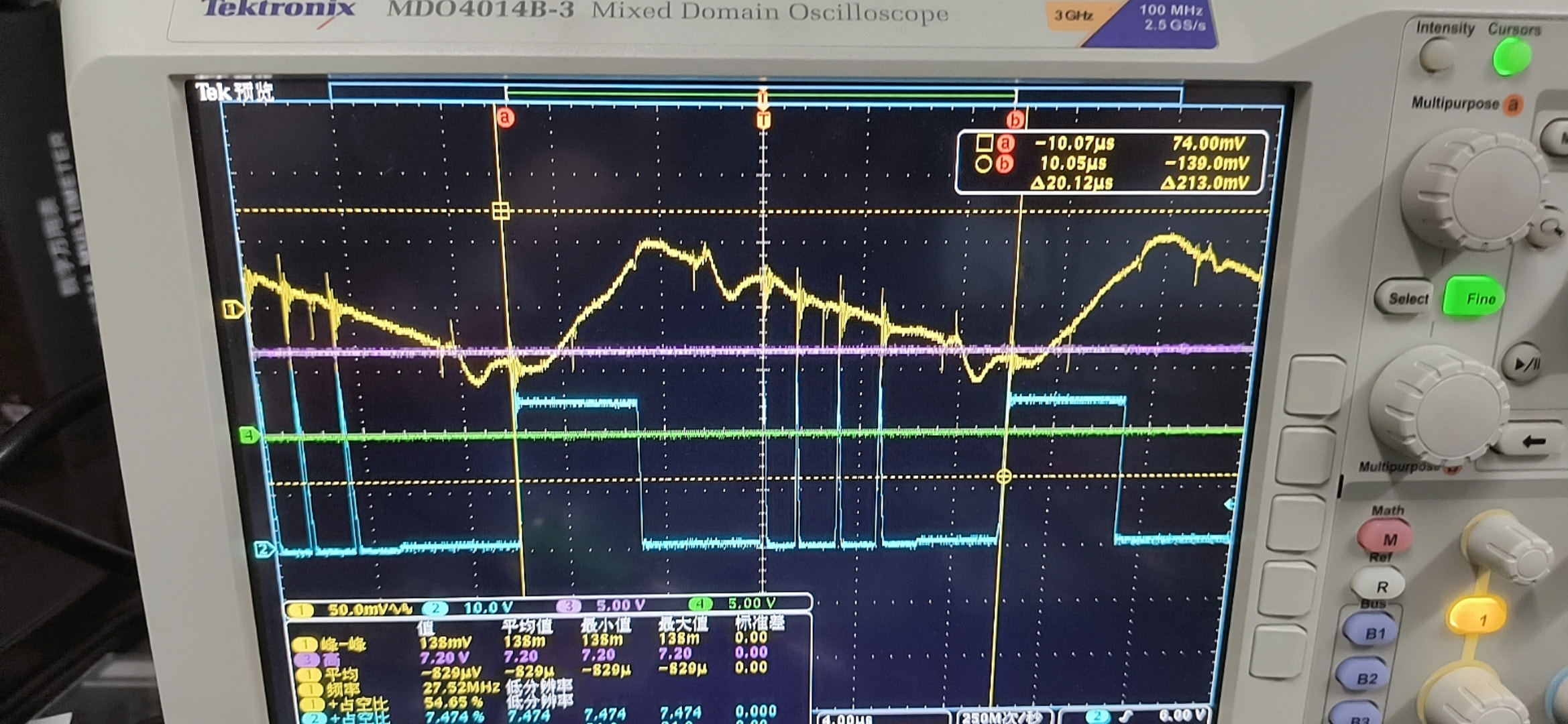
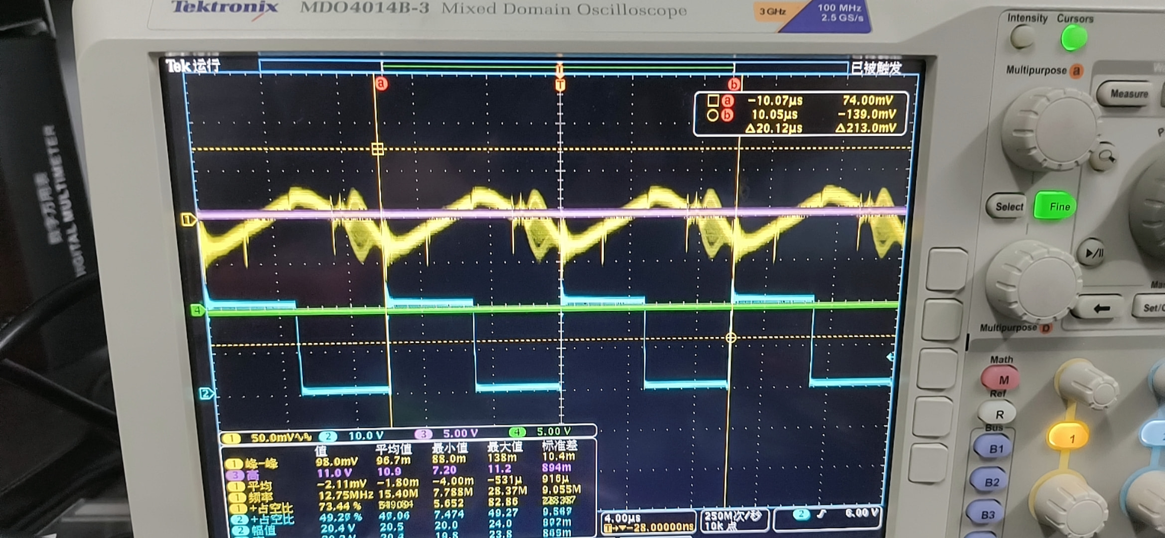
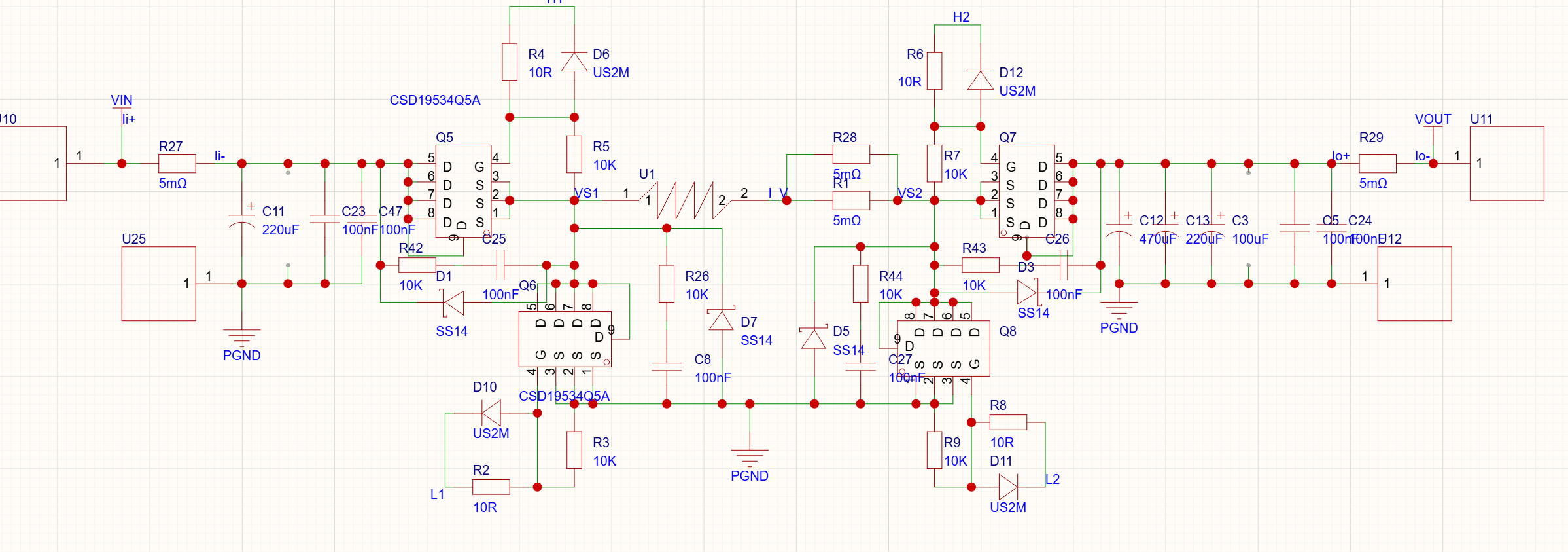
The first image is my schematic, the second is the BUCK-side VS-to-ground and inductor current waveforms when testing above 20V, the third is a zoomed-in view of the second, and the fourth is the VS and inductor current below 20V. My PWM is 100K with a fixed duty cycle of 0.5.
-
Why does increasing the input voltage cause the inductor current ripple frequency to decrease, and why does VS become a very spiky waveform instead of a square wave when the MOSFET turns on the second time?
-
How can I solve this problem?
In constant voltage mode with a 5V output, when the electronic load is off, the output voltage is 5V. When the electronic load is set to 0.5A, the electronic load displays the output voltage as 4.91V; when set to 1.5A, it displays 4.74V; and when set to 2.5A, it displays 4.56V. However, under all of the above conditions, the MCU’s sampled output voltage remains at 5V. What could be the reason for this?
Voltage drop due to line loss—is the wire connecting your electronic load too thin?
It’s definitely related to wire loss. I’m using 14 AWG wire, but it seems like your video demo wasn’t affected by it. How did you manage that?
Then check if the voltage at the terminal block on the power supply board has dropped.
Bro, I checked the schematic and waveforms you posted. This phenomenon is super classic when building STM32 digital power supplies (especially your own discrete-driven Buck-Boost).
Since you’ve hard-coded the PWM to a fixed 50% (0.5) duty cycle in your program, theoretically the MCU should be spitting out an equal-width square wave relentlessly. What you’re seeing in Figure 3 (>20V)—“alternating wide and narrow pulses”, “chaotic inductor current ripple frequency (Pulse Skipping / uneven pulses)”, and “extremely narrow spikes at the VS node”—is fundamentally caused by the drive signal for that cycle being abnormally truncated.
Let me walk you through the causes and troubleshooting ideas based on my experience:
1. Why does this phenomenon occur after the voltage goes up?
When the input voltage rises from <20V to >20V, the most direct change is that the dv/dt and di/dt during switching actions increase significantly. This triggers several fatal chain reactions:
-
Interference/Ground Bounce causing MCU or drive logic confusion: After the voltage increases, the high-frequency noise (EMI) during switching moments becomes stronger. This noise can easily couple into the MCU’s PWM traces, or cause severe jitter in the reference ground level. If the logic input of the driver IC reads a glitch, or the MCU timer is interfered with, the PWM that should have lasted for half a cycle will be turned off prematurely, forming the “spike” you see.
-
Bootstrap circuit failure or excessive negative voltage at VS: Your schematic uses a high-low side driver scheme with bootstrap capacitors (C25, C27, currently looking like 100nF). When the voltage increases, the inductor freewheeling current during the dead time causes very deep negative voltage ringing at the VS node (below PGND). If the negative voltage goes too deep, it will instantly suck the charge out of the bootstrap capacitor, or trigger the driver IC’s internal undervoltage lockout (UVLO). Once the bootstrap voltage drops, the high-side immediately shuts down, turning into an extremely narrow spike.
-
Hardware protection false triggering (if applicable): If your board has hardware overcurrent protection or an op-amp comparator based on current sensing (like the 5mΩ resistors R27, R28 in the diagram), after the voltage increases, the “Leading Edge Spike” at the switching moment will also get larger. This can very easily cause the comparator to falsely trip, forcibly masking the current PWM pulse.
-
Inductor tending towards saturation: Although it might not be the main cause, increased voltage leads to higher peak currents. If the inductor doesn’t have enough margin, the spikes brought by the soaring current will also exacerbate the aforementioned noise interference.
2. How to troubleshoot and fix it?
Don’t rush to re-spin the board; debugging digital power supplies is all about “following the trail”. I suggest you follow these steps:
Step 1: Identify who the “culprit” really is (most crucial!)
Right now you’ve only probed the VS node. You need to take two oscilloscope channels and simultaneously probe the STM32’s PWM output pin and the VS node (or the high-side Gate pin).
-
Scenario A: If the waveform measured at the MCU pin is already alternating wide and narrow or a complete mess, it means the high-power side is interfering with the MCU. You need to check if the STM32’s power supply is stable, if the grounds for the high and low voltage sides are properly poured/single-point grounded, or try adding a small RC filter near the PWM at the driver IC (e.g., a few tens of ohms in series with a 22pF capacitor to ground).
-
Scenario B: If the MCU pin is outputting a perfect 50% square wave, but the VS end still shows spikes, then the problem lies in the driver stage. Focus on Step 2 below.
Step 2: Optimizing the driver stage
If it’s a driver-side issue, it’s highly likely caused by the bootstrap or switching speed being too fast:
-
Increase the bootstrap capacitor: Your current C25 and C27 are 100nF, which might be a bit sketchy when running at a 100k frequency under heavy load or high voltage. I recommend paralleling a 1uF MLCC to ensure the high-side has enough charge to stay on.
-
Suppress switching node ringing (key point): Zoom in on the falling edge of the waveform with your oscilloscope. Does the VS node dip to -2V or even lower? If so, I suggest adding an RC Snubber (RC absorption circuit) from VS1 to ground and VS2 to ground (e.g., a few ohms resistor in series with a few hundred pF capacitor) to absorb the ringing.
-
Slow down the switching speed slightly: You can series a small resistor at the high-side Gate (if there’s room; looking at the schematic, it seems directly connected). Sacrifice a little bit of switching loss to reduce the dv/dt, and the whole system will be much more stable.
-
Check diode reverse recovery: Your bootstrap diode uses an SS14 (Schottky) with a 40V withstand voltage. When the input is >20V, if you add ringing, the reverse voltage tolerance might be a bit marginal. I recommend swapping it for a diode with a higher voltage rating and extremely fast recovery, and adding a small resistor of around 2.2Ω in series to limit the peak charging current.
Go probe the PWM source at the MCU pin first. Once you confirm whether the source is being interfered with or the driver stage just can’t handle it, you can prescribe the right remedy. Happy debugging!
I looked at your waveforms and schematic, and this phenomenon is quite typical. The core reason is that after the input voltage increases, the inductor enters Discontinuous Conduction Mode (DCM).
1. Why does increasing the input voltage reduce the ripple “frequency,” and why is the second turn-on VS a sharp pulse instead of a square wave?
The PWM frequency actually hasn’t changed; it’s still 100K. This is a visual effect caused by the deformation of the current waveform.
You are currently in open-loop with a fixed 50% duty cycle, so in pure Buck mode, the output is roughly half the input. As the input voltage increases, the inductor current ripple ΔI = (Vin-Vout)×D/(L×f) will increase linearly. When the peak-to-peak ripple exceeds twice the average output current, the valley current hits 0 directly, dropping from CCM into DCM.
After entering DCM:
- During the turn-off phase, the inductor current drops to 0 early, the freewheeling diode stops conducting, and the VS node becomes high-impedance. It undergoes free resonance with the parasitic LC, so it is no longer clamped into a square wave.
- When the MOSFET turns on again in the next cycle, the inductor current is 0, which is equivalent to hard-switching — the MOSFET directly charges and discharges the parasitic capacitance of the switching node, causing an extremely high di/dt and producing a very sharp voltage pulse. However, because there is no sustained inductor current to maintain it, the spike dissipates quickly, so it looks like a narrow pulse instead of a square wave plateau.
- The so-called “reduced ripple frequency” is actually because the current stays at 0 for more than half the cycle (with only tiny resonant fluctuations), and the effective triangle wave only occupies a small portion; visually, it looks like the frequency has decreased. In severe cases, a pulse-skipping phenomenon can occur where energy is only transmitted every other cycle.
Also, since you are using a bootstrap-driven high-side NMOS, VS doesn’t go to ground for a long time under DCM. The bootstrap capacitor C7 cannot charge, which degrades the driving capability and makes the turn-on waveform look even worse — on your schematic, C7 is labeled 100pF, which is also too small. Bootstrap capacitors generally start at several hundred nF.
2. How to fix it?
Here are a few directions, ranked by priority:
① Return to CCM (Addressing the root cause)
- Switch to an inductor with a larger inductance: Calculate based on the maximum input voltage to ensure the peak-to-peak ripple does not exceed 30%~40% of the average current, leaving enough margin. This is the most direct approach.
- Increase the load: Raising the average output current “lifts” the valley current away from 0, which can quickly verify if it’s a DCM issue.
- Reducing the switching frequency can also decrease the ripple, but 100K is quite reasonable, so it’s not recommended to change the frequency.
② Suppress spikes and ringing (Improving stress and EMI)
- Add an RCD snubber from the VS node to ground (e.g., a 100Ω resistor + 1nF capacitor + fast recovery diode), or a simple RC snubber (tens of Ω + hundreds of pF). This can significantly suppress the spikes and ringing.
- In the layout, minimize the copper area of the switching node and route the drive loop with the shortest path to reduce parasitic parameters.
③ Control method improvement
- Open-loop fixed duty cycle isn’t very suitable for topologies like Buck-Boost to begin with. It’s recommended to switch to closed-loop voltage control, where the duty cycle adjusts automatically when the input changes, which both regulates the voltage and mitigates DCM issues.
- If you must run open-loop, then redesign the inductor parameters based on your maximum input voltage to ensure CCM across the entire range.
To summarize: The essence is that high voltage and light load caused it to drop into DCM, and the spikes are a product of zero-current hard-switching. You can try temporarily connecting a heavy load first. If the waveform recovers to the square wave + triangle wave like it was at low voltage, then you’ve confirmed DCM is the problem, and you can just swap in a larger inductor.
Measured with a multimeter, the voltage does drop; it’s not exactly 5V. But measuring the wire impedance with a multimeter shows around 180mΩ, which matches up with the magnitude of the voltage drop when the current is increased.