A Four-Switch Buck-Boost Digital Power Supply Based on STM32G474, Supporting TypeC Interface PD Fast Charging Input and DC5.5 Interface Input, with Input/Output Maximum 48V10A. This is my graduation project, now open-sourced, including schematics, PCB, program source code, shell 3D models and other materials.
The work is mediocre, no harsh criticism please, friendly discussion is welcome.
Project Demo Video: https://www.bilibili.com/video/BV1Ui421y7ip/
Intelligent Electronic Load Based on CH32V307 Open Source, Embedded Competition Project Open Source: https://blog.zeruns.com/archives/785.html
This project’s open-source link on the Lichuang Open Source Platform: https://url.zeruns.com/noGf0
Electronics/Microcontroller Technology Exchange QQ Group: 2169025065
Material download address is at the end of the article.
The hardware circuit design uses Lichuang EDA software, which is really easy to use.
Introduction
This article designs a synchronous rectification Buck-Boost digital power supply based on STM32. The power supply circuit consists of MOSFET driver circuit, 4-switch Buck-Boost circuit, signal conditioning circuit, PD fast charging protocol circuit, auxiliary power circuit, microcontroller control circuit and other components.
The power supply can be powered through a DC interface or Type-C interface, and the Type-C interface supports communication with chargers through PD fast charging protocol, automatically requesting and obtaining a maximum working voltage of 20V. The power supply uses STM32G474 microcontroller to monitor input and output voltage and current in real-time, and adjusts the output PWM duty cycle through PID control algorithm, achieving overvoltage and overcurrent protection. It can also sample the motherboard temperature to achieve overtemperature protection. Additionally, power supply parameters can be viewed in real-time through an OLED screen, and output voltage and current can be set through a rotary encoder and buttons. Communication with a host computer can also be achieved through another Type-C interface. Through the host computer software, various parameters and waveforms of the power supply can be viewed in real-time.
Design Performance Parameters
The power supply design performance parameters are as follows:
| Item | Parameter |
|---|---|
| Input Voltage Range | 12Vdc~48Vdc |
| Input Current Range | 0~10A |
| Maximum Output Power | 450W |
| Output Voltage Range | 0.5Vdc~48Vdc |
| Output Current Range | 0~10A |
| Output Voltage Ripple | Peak-to-peak ≤200mV |
| Switching Frequency | 181.333kHz |
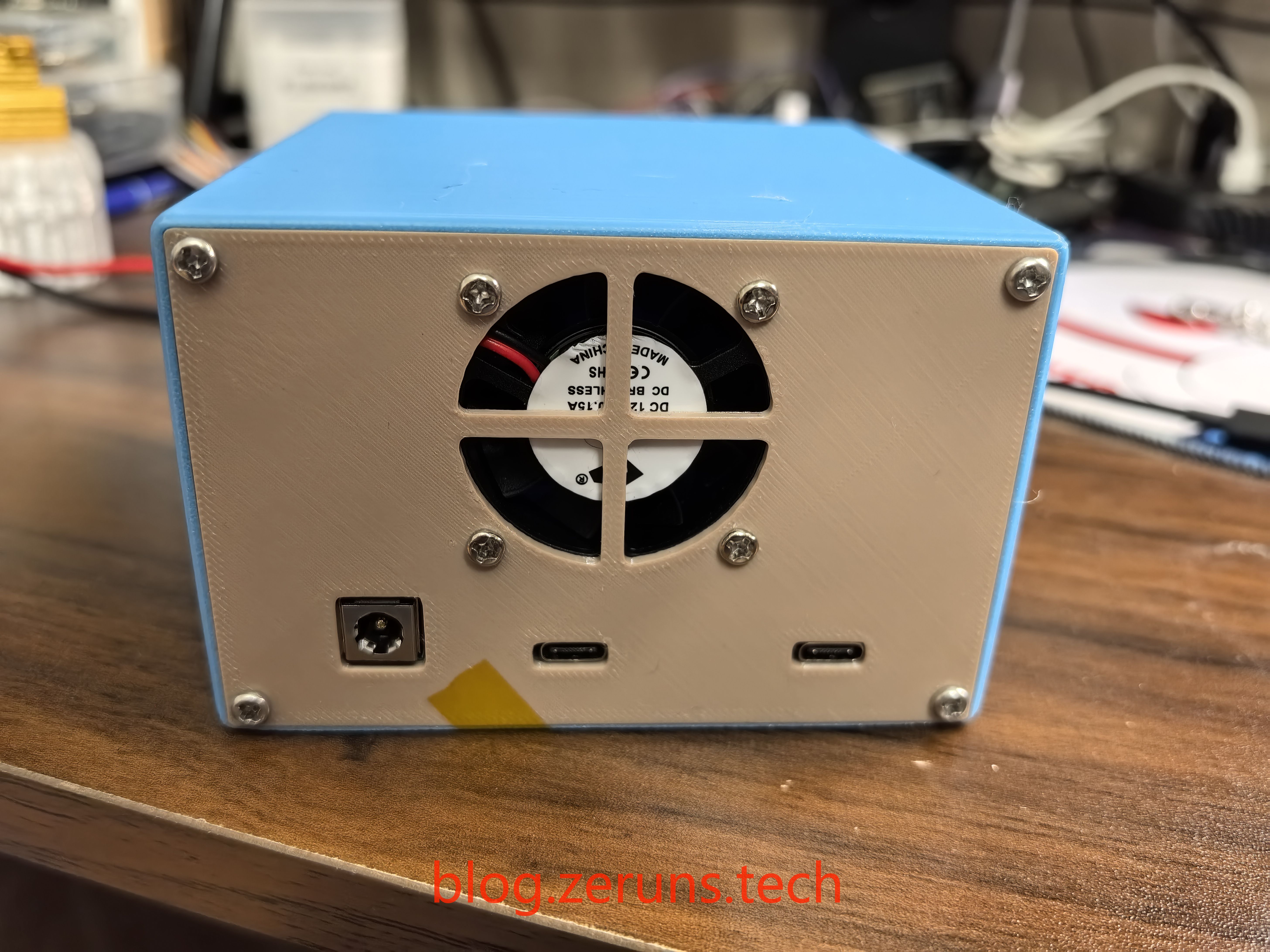
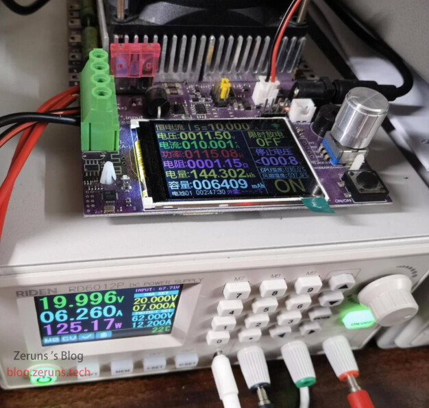
Physical Photos
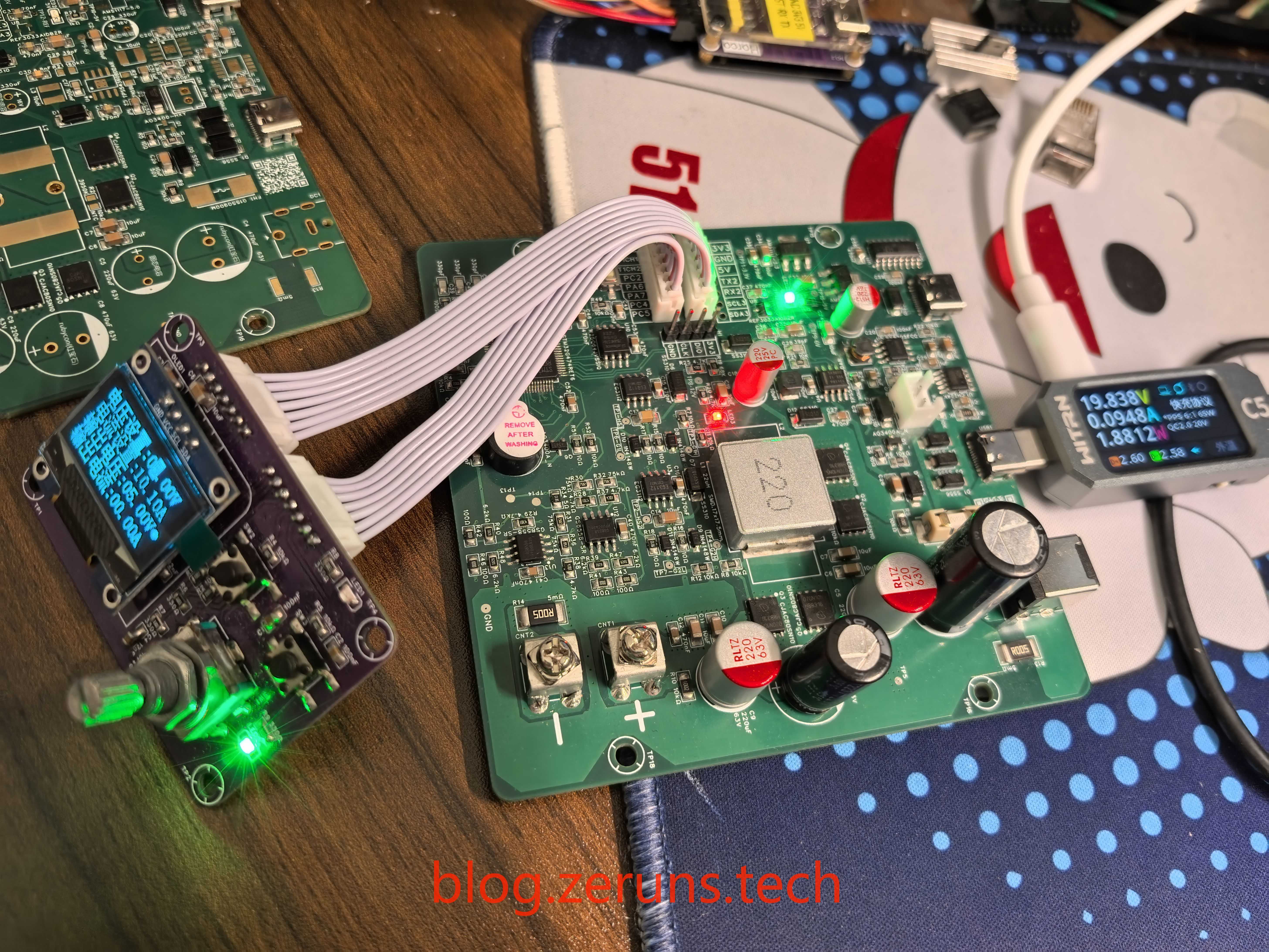
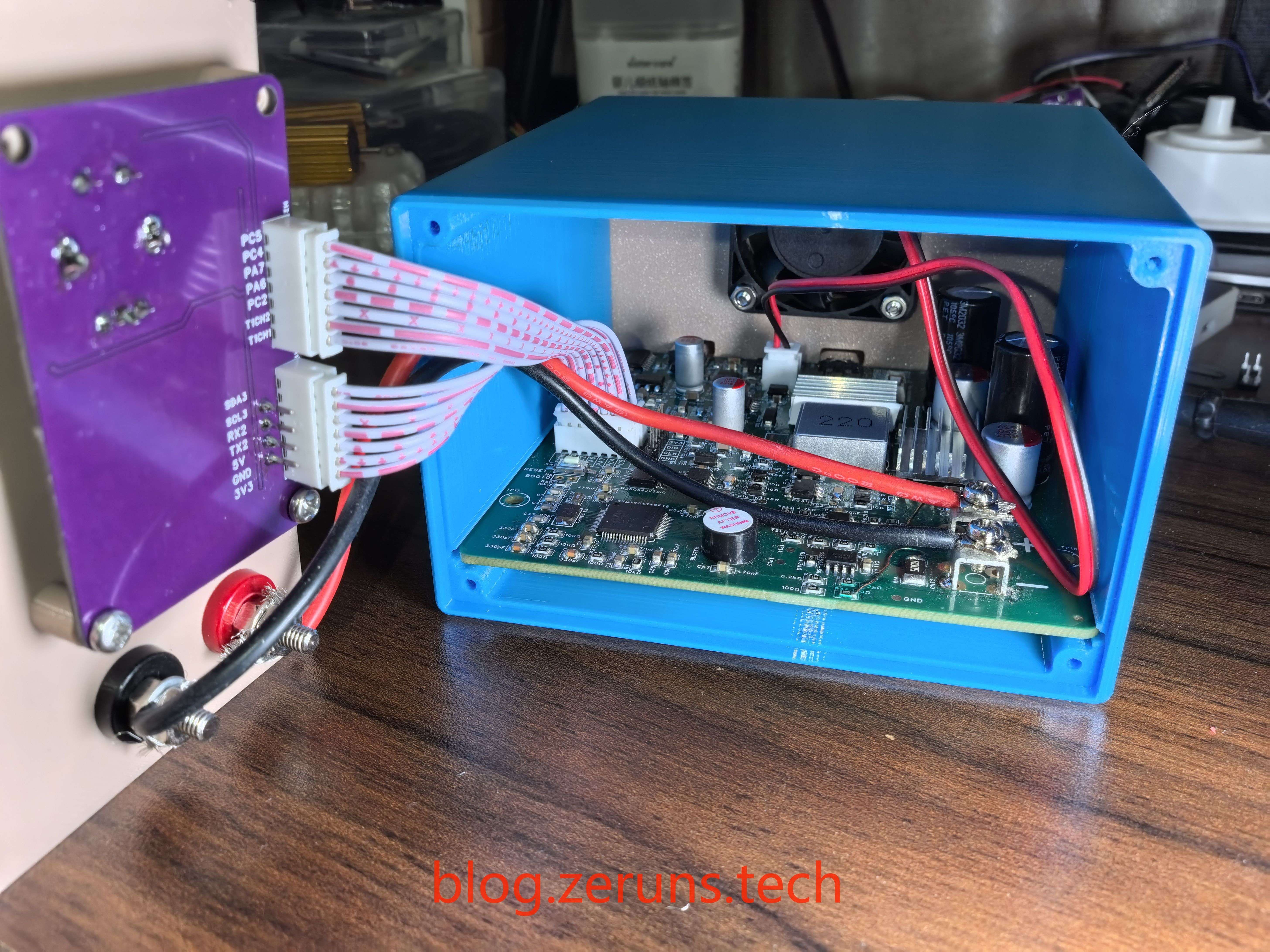
![]()
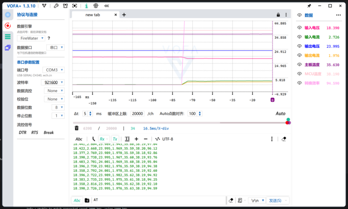
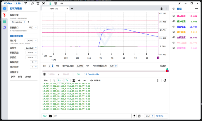
Using VOFA+ as the host computer software, you can view the power supply’s various parameters in real-time (input voltage and current, output voltage and current, motherboard temperature, MCU temperature, power conversion efficiency, etc.) and waveform changes. As shown in the following figures.
System Block Diagram

Hardware Circuit Design
Component Selection and Calculation
Inductor Calculation
In a synchronous BUCK-BOOST power supply, inductor calculation needs to consider the operating conditions in both BUCK and BOOST modes to ensure the circuit meets working requirements in both modes. Typically, inductor selection is based on the mode with higher inductor requirements.
When the power supply operates in BUCK step-down mode, assuming maximum input voltage is 48V and minimum output voltage is 5V, calculate the minimum PWM duty cycle:
Define the inductor current ripple (25% of maximum rated current ripple, with maximum rated current of 10A):
Calculate the minimum required BUCK inductor:
When the power supply operates in BOOST step-up mode, using the nominal input voltage of 24V as the calculation point, calculate the PWM duty cycle:
In Boost mode, when taking 1A (I_{minb}) for Boost to enter continuous mode (CCM), calculate the inductor:
Based on the calculation results from the formulas, the minimum inductor value required to meet the predetermined ripple current requirements has been determined. To ensure this condition is met, an inductor with a value slightly higher than the calculated value should be selected. At the same time, it must be ensured that the saturation current of the selected inductor can handle the highest current peak in the circuit. Since efficiency factors were not considered in the calculation process, the actual duty cycle and peak current may be lower than theoretical calculated values. Therefore, when making selections, a certain safety margin should be considered to adapt to various situations that may occur under actual working conditions.
Considering all the above factors, this design uses a 22μH inductor with 1770 surface mount package and saturation current above 10A as the inductor element for the BUCK-BOOST circuit.
Capacitor Calculation
To achieve good output voltage ripple, the design voltage ripple is set to 50mV.
The inductor selected above is 22μH, so this calculation also uses this inductor value:
Calculate the minimum capacitance required when operating in BUCK step-down mode and BOOST step-up mode respectively, C_{minBuck} and C_{minBoost}:
The design requires a certain margin, and for lower output ripple, one 220μF low-ESR solid-state capacitor and one 470μF ordinary electrolytic capacitor are selected, totaling 690μF.
MOSFET Selection Calculation
Within the rated input and output voltage range, the RMS current of the input MOSFET is calculated as:
In MOSFET selection, the rated current value I_D of the MOS tube should be at least 2 times the maximum current flowing through the MOS tube (to prevent impact damage from excessive current in fault or short-circuit conditions).
The rated voltage withstand value V_{DS} of MOSFET selection should be greater than 1.5 times the maximum input voltage (to prevent spike breakdown):
After referring to the previous calculations, for conventional application scenarios, a MOSFET with rated current exceeding 15 amperes (A) and voltage rating of 100 volts (V) can be selected. The lower MOSFET selection is the same as the upper MOSFET. Considering heat generation, to minimize energy loss during conduction and switching, MOSFETs with low on-resistance (R_{DS(on)}) and low output capacitance (Coss) should be prioritized.
This design uses the MOSFET model CJAC80SN10, manufactured by Jiangsu Changjing Technology Co., Ltd., a domestically produced MOSFET. It features a drain-source voltage (V_{DS}) of 100V and maximum drain-source current (I_D) of 80A. Its on-resistance (R_{DS(on)}) is only 6.2mΩ, which helps reduce power loss when the device is conducting. Meanwhile, the device’s output capacitance Coss has a typical value of 420pF, which helps reduce dynamic loss during switching conversion. Therefore, CJAC80SN10 meets the project’s electrical requirements while effectively reducing energy loss and improving overall system efficiency.
Power Board Circuit Design
Main Power Circuit
The figure below shows the synchronous BUCK-BOOST power supply main power circuit diagram. The left side is the input. The synchronous BUCK step-down circuit consists of MOS tubes Q2 and Q4 with inductor L1. The synchronous BOOST step-up circuit consists of MOS tubes Q3 and Q5 with inductor L1. Each MOS tube has a 10kΩ resistor connected between the gate and source to ensure the MOS gate is not floating, preventing malfunction and unintended conduction.
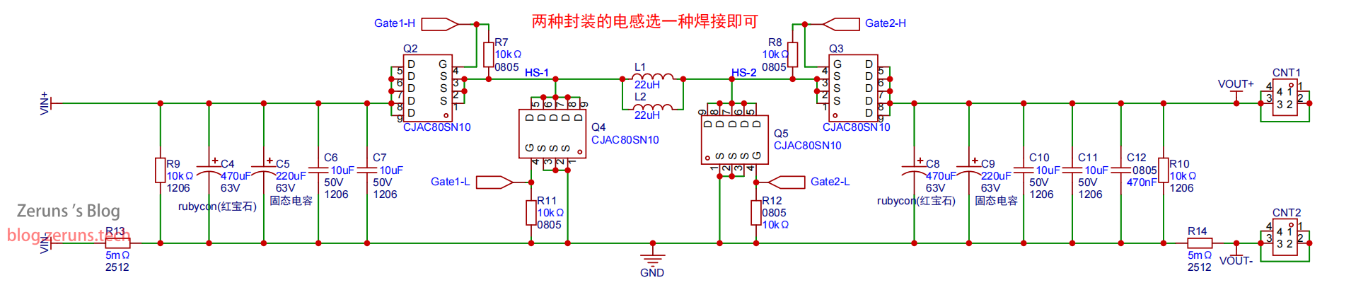
The main power circuit has a left-right symmetric structure overall. Both input and output ends are equipped with one 470μF/63V aluminum electrolytic capacitor and one 220μF/63V solid-state aluminum electrolytic capacitor. Additionally, there are 2 small surface mount MLCC (multilayer ceramic capacitors) with parameters of 10μF/50V to filter high-frequency noise interference at the ports. R9 and R10 serve as dummy loads at the input and output ports, allowing rapid dissipation of residual energy in the circuit when the power supply is disconnected. R13 and R14 are high-precision 5mΩ resistors used for current sampling, with a differential amplification circuit in the next stage to amplify the input and output current signals. CNT1 and CNT2 are output terminals. L1 and L2 are surface mount 1770 package and through-hole ferrite core inductor packages respectively; only one needs to be soldered, both are drawn for convenience in testing the effects and performance of different inductors.
Power Input and Fast Charging Protocol Circuit
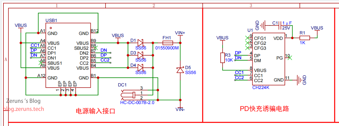
The figure below shows the power input interface and PD fast charging protocol communication circuit diagram.
The power supply input uses two types of interfaces: DC5.5*2.5mm female connector and Type-C female connector. The Type-C interface supports BC1.2, PD3.0/2.0 and other fast charging protocols. The fast charging protocol chip model used is CH224K, which can communicate with fast charging chargers to make them output a maximum voltage of 20V, supporting up to 100W power.
Diodes D1, D3, and D4 prevent voltage backflow from the DC interface to the Type-C interface. The design does not allow both interfaces to be connected simultaneously. D5 is a diode for reverse polarity protection. FH1 is a power input fuse holder with a 12A fuse.
Driver Circuit
In the design of synchronous BUCK-BOOST power supplies, both the BUCK circuit and BOOST circuit contain high-side N-MOSFETs. Traditionally, driving these high-side N-MOSFETs typically uses transformer-isolated drive methods, but this approach increases circuit complexity and expands the circuit board size.
This design uses two MOS driver chips EG3112 with built-in bootstrap circuit functions to drive the MOS tubes of the BUCK and BOOST circuits. EG3112 is a non-isolated complementary dual-channel driver chip. Its 2A output drive current capability ensures that the MOSFET can conduct quickly. The chip also has built-in dead-time control function to prevent direct conduction of output drive signals, improving system stability. The specific circuit is shown in the figure below.
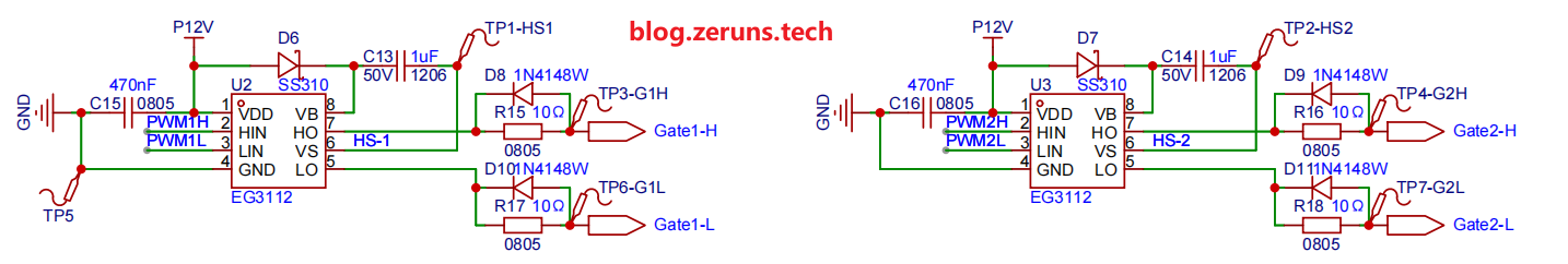
Taking the BOOST step-up circuit MOS driver as an example, PWM2L and PWM2H are PWM signals output from the STM32G474 microcontroller, sent to the LIN and HIN pins of the EG3112 driver chip. LO is the lower tube drive signal output with drive resistor value of 10Ω. HO is the upper tube drive signal output with drive resistor value of 10Ω. D7 is the upper tube drive circuit bootstrap diode. D9 and D11 diodes are used for rapid gate charge release to speed up MOS tube turn-off. C14 is the bootstrap capacitor.
The drive resistor functions to reduce reflections and oscillations that may occur on PCB traces, distributed capacitances, inductances and other components during MOSFET switching. By connecting a series resistor, such oscillations can be reduced, improving system stability and reliability.
Auxiliary Power Supply
The figure below shows the schematic diagram of the power board auxiliary power supply circuit.
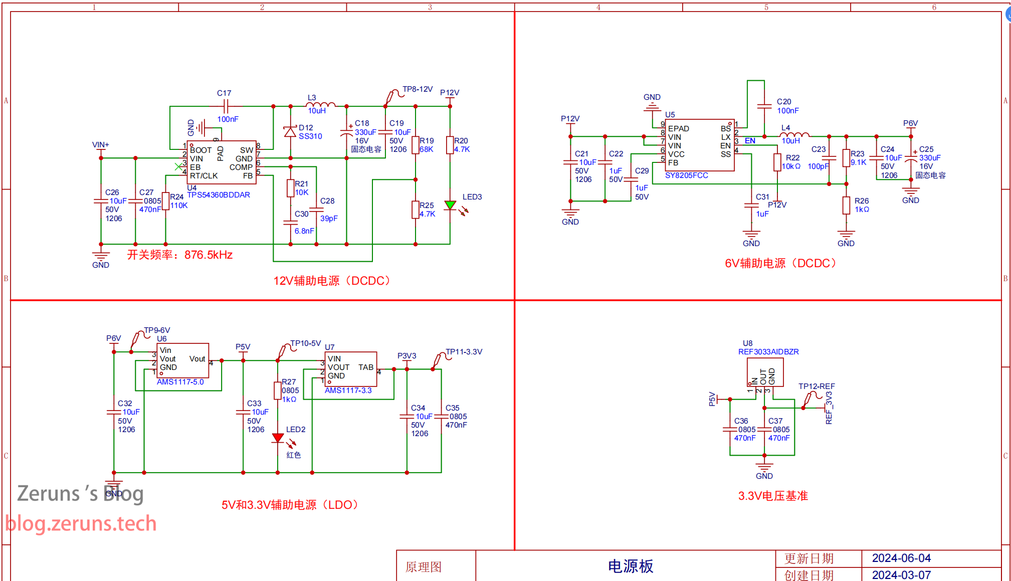
The first stage 12V output auxiliary power circuit uses the BUCK-type power chip TPS54360B with integrated high-side MOSFET. According to the chip manual, connecting a pull-down resistor to the RT pin can set the switching frequency. Here a 110kΩ resistor is selected, corresponding to a switching frequency of 876.5kHz. The higher switching frequency allows selection of a smaller inductor to save space. Based on this frequency, the inductor value should be greater than 9.75μH. Here a 10μH inductor is selected, with SS310 as the freewheeling diode. C26 and C27 are input filter capacitors. Feedback voltage divider resistors R19 and R25 divide out a 0.8V reference voltage to the chip’s FB pin to ensure output voltage is 12V. C18 and C19 are filter capacitors for the first stage 12V output auxiliary power supply. The first stage 12V output mainly supplies the input of the second stage 6V step-down circuit, as well as MOSFET driver circuits and cooling fans.
The second stage 6V output auxiliary power circuit uses the synchronous rectification BUCK-type power chip SY8205 with integrated MOSFET. According to the chip manual, the chip switching frequency is fixed at 500kHz. The inductor for the auxiliary power BUCK circuit is selected as 10μH. C21 and C22 are input filter capacitors. Feedback voltage divider resistors R23 and R26 divide out a 0.6V reference voltage to the chip’s FB pin to ensure output voltage is 6V. C24 and C25 are filter capacitors for the second stage 6V output auxiliary power supply. Since directly using a linear regulator to step down from 12V to 5V would cause significant loss, a switching power supply is first used to step down to a voltage close to 5V, then a linear regulator steps down to the target voltage. This ensures high efficiency and low output ripple.
The 6V output from the second stage is stepped down to 5V through the linear regulator chip AMS1117-5 as the third stage auxiliary power supply, with voltage reference chip REF3033 supplying signal conditioning, OLED display, USB communication and other functional circuits.
The 5V DC is stepped down to 3.3V through the linear regulator chip AMS1117-3.3 as the fourth stage auxiliary power supply, supplying MCU, buzzer, Flash chip and other circuits.
The voltage reference chip REF3033 outputs a 3.3V reference voltage to the MCU’s VREF port for use as the reference voltage for the MCU’s built-in ADC, improving ADC sampling accuracy.
Signal Conditioning Circuit
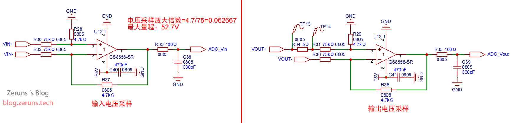
As shown in the figure above, the input and output voltage sampling and signal conditioning circuit in this design uses differential amplification technology. The differential amplification topology can effectively reduce the interference of high-frequency noise in switching power supplies on the signal conditioning circuit, improving signal stability and reliability. In this circuit, the low offset voltage operational amplifier GS8558-SR is selected to enhance conversion accuracy. The GS8558-SR op-amp has excellent DC accuracy and low bias current characteristics, which are critical to improving the performance of the entire signal conditioning circuit.
Feedback resistors for the differential amplification circuit:
Calculate the differential amplification gain:
The MCU’s ADC maximum sampling voltage is 3.3V output by the voltage reference chip. The maximum input and output voltage that can be sampled is calculated as:
To better suppress high-frequency noise interference from switching power supplies on the differential amplification circuit, decoupling capacitors C40 and C41 are added to the op-amp power pins for filtering. The capacitors are selected as MLCC (multilayer ceramic capacitors). MLCC has lower ESR and ESL, providing better filtering effects for high-frequency noise. Meanwhile, resistor R35 and capacitor C39 at the output form an RC low-pass filter circuit to filter out high-frequency noise.
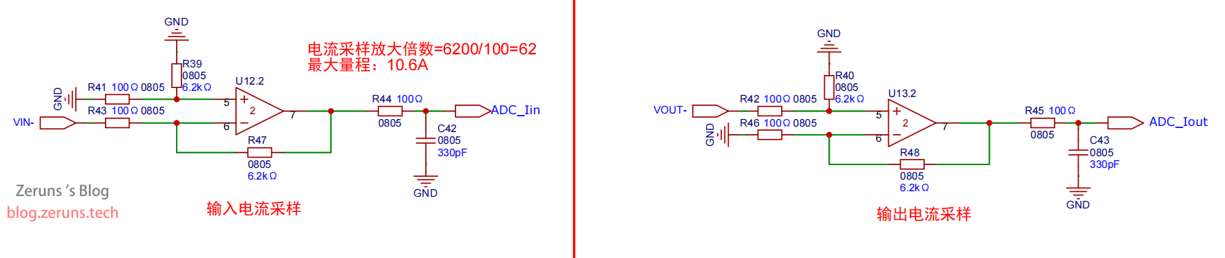
As shown in the figure above, the input and output current conditioning circuit uses differential amplification. The output current sampling resistor is:
Feedback resistors for the differential amplification circuit:
Calculate the differential amplification gain:
That is, each 1A of current outputs 310mV of voltage.
The MCU’s ADC maximum sampling voltage is 3.3V output by the voltage reference chip. The maximum input and output current that can be sampled is calculated as:
MCU Control Circuit
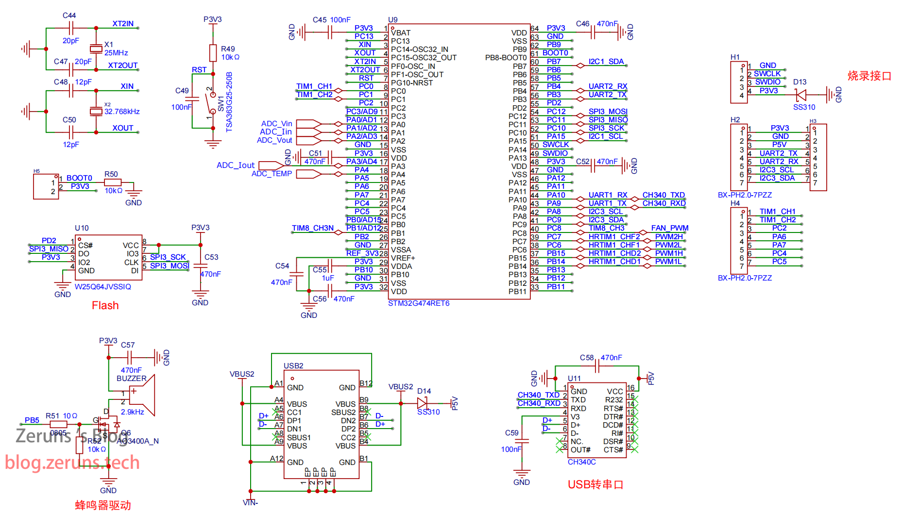
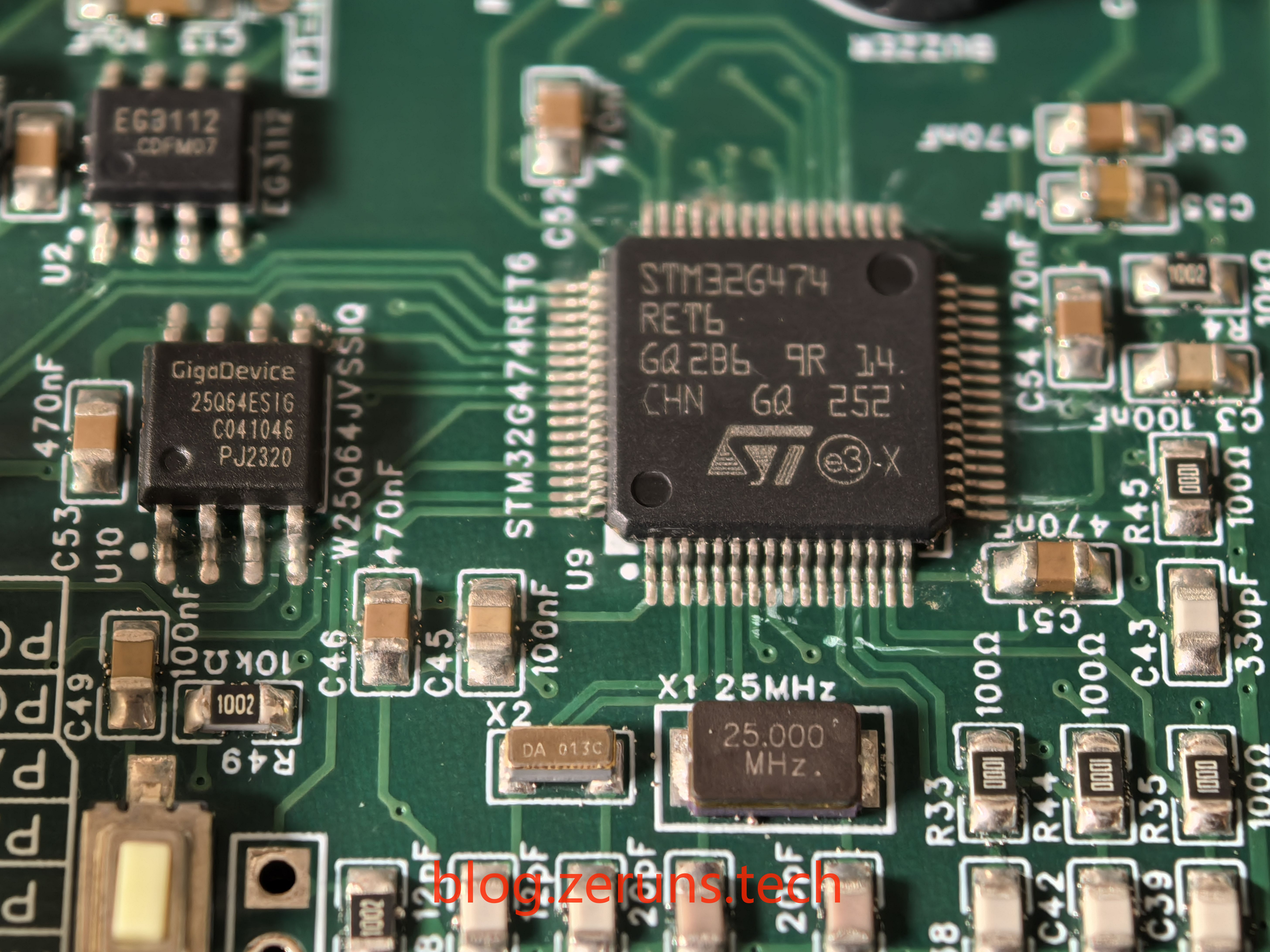
This digital power supply design uses the STM32G474RET6 chip as the controller, which has the outstanding characteristics of simple peripheral circuits, diverse control methods, and superior expansion capabilities. To achieve precise clock signals, the controller uses an external crystal oscillator X1, which is a 25 megahertz (MHz) quartz crystal oscillator. Additionally, the circuit includes multiple filter capacitors, including C45, C51, C56, C46, and C52, which are respectively used for different digital power pins of the microcontroller (MCU) to ensure power stability and reduce noise interference. Resistor R49 and capacitor C49 form a power-on reset circuit. SW1 is the MCU reset button. U11 is a USB-to-serial chip with model CH340C, connected to the second Type-C interface, with the serial port connected to the MCU’s USART1 interface. U10 is a Flash storage chip with model W25Q64, used to store parameter settings and other information, connected to the MCU’s SPI3 interface. Q6 is a buzzer drive MOS tube for controlling the buzzer, with the MOS gate connected to the MCU’s PB5 port. H1 is a SWD programming port. H2 and H4 are PH2.0 connectors for connection with the control panel. The connectors have a USART2 interface reserved, allowing convenient replacement of the control panel scheme with a serial port screen. An ESP32 can also be added to increase networking and wireless control functions. D13 is a 5V reverse polarity protection diode.
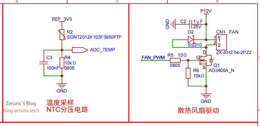
Cooling Fan Drive and Motherboard Temperature Sampling Circuit
The motherboard temperature sampling circuit and cooling fan drive circuit schematic diagram is shown in the figure below. The principle of motherboard temperature sampling is to use an NTC thermistor R2 connected in series with a pull-down resistor R4 to divide the voltage and output to the MCU’s ADC port for sampling. The NTC thermistor used has a resistance value of 10kΩ and a B value of 3950K.The cooling fan is driven by an N-MOS transistor with the model number AO3400. A diode D2 is connected in reverse parallel at the cooling fan interface to prevent damage caused by the back EMF (back electromotive force) generated by the motor. When the motor loses power, due to rotational inertia, the motor rotor will not stop immediately but will continue to rotate and generate an electromotive force. This electromotive force may damage transistors or integrated circuits in the circuit, especially when the motor is connected to these components through a semiconductor switch (such as a MOSFET).
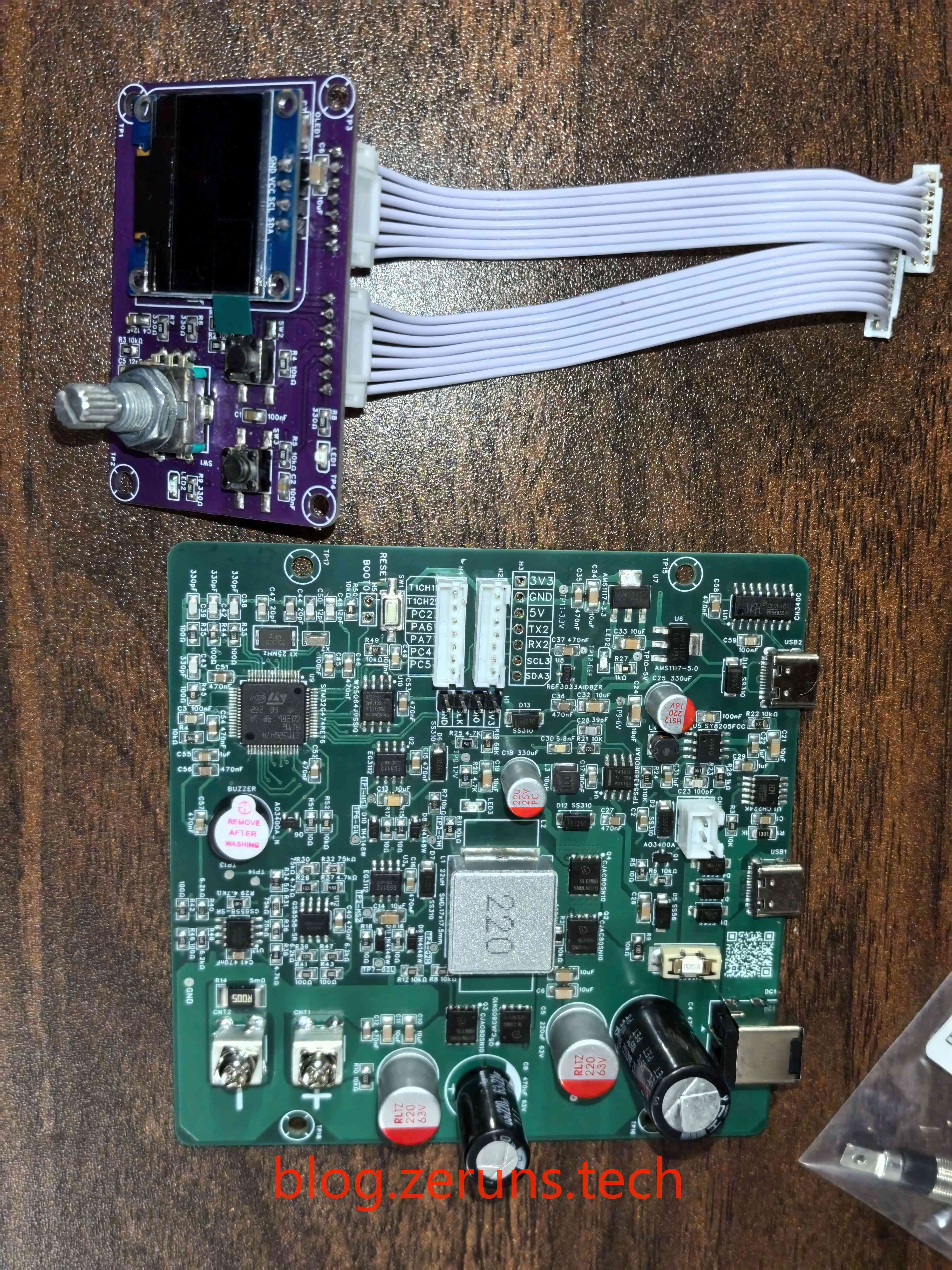
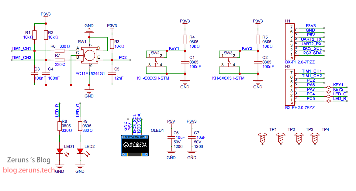
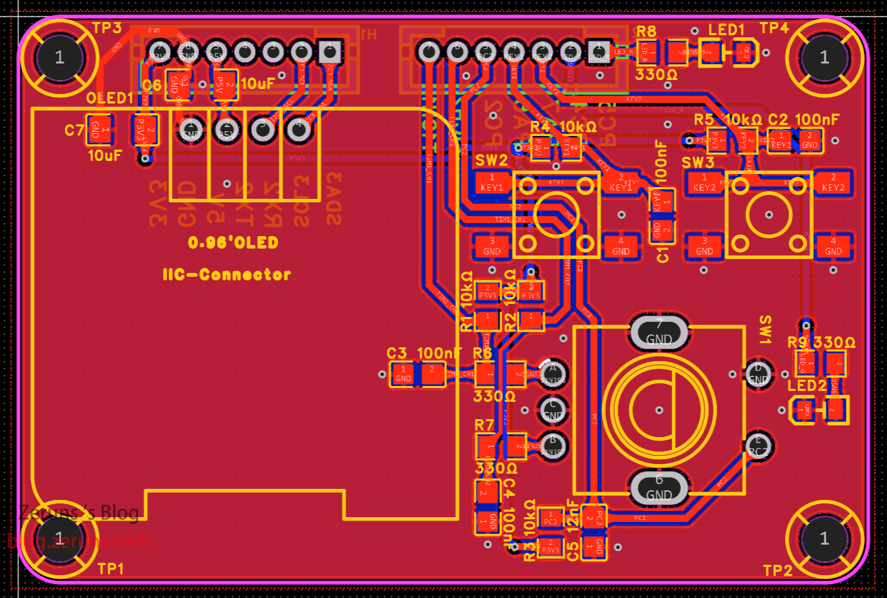
Control Panel Circuit Design
The circuit schematic of the control panel is shown in the figure below. SW1 is a rotary encoder used for parameter settings, etc. SW2 and SW3 are buttons. SW2 is used to switch between setting items, and SW3 is used to control the on/off of the power output. LED1 is the system running status indicator light, which flashes at 500ms intervals during normal operation. LED2 is the output status indicator light, which lights up when the output is on and turns off when the output is off. OLED1 is an OLED screen used to display power parameters, status information, and other details.
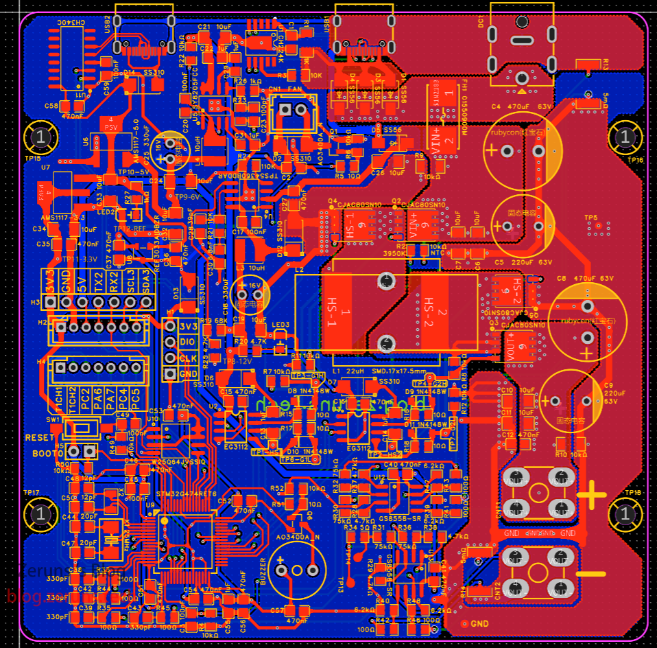
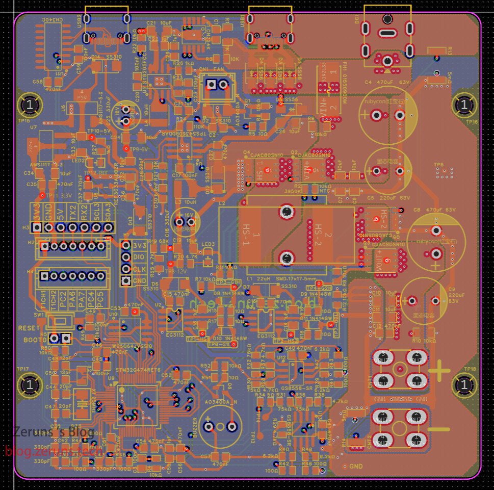
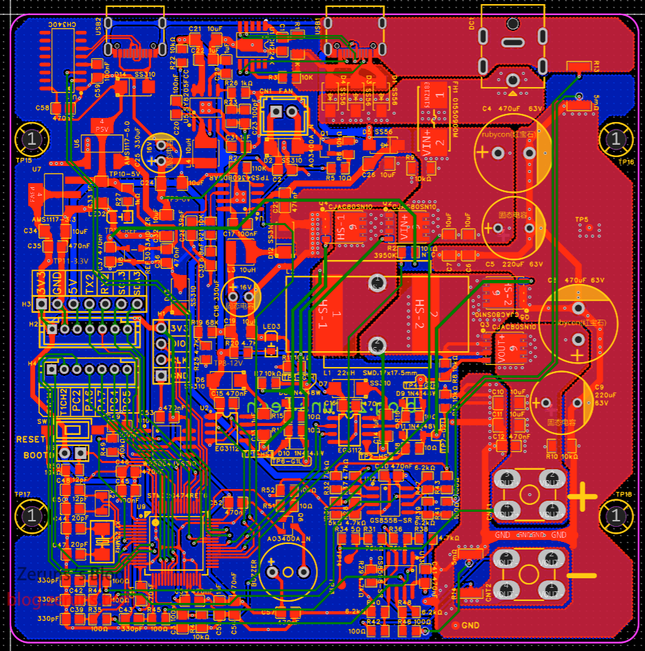
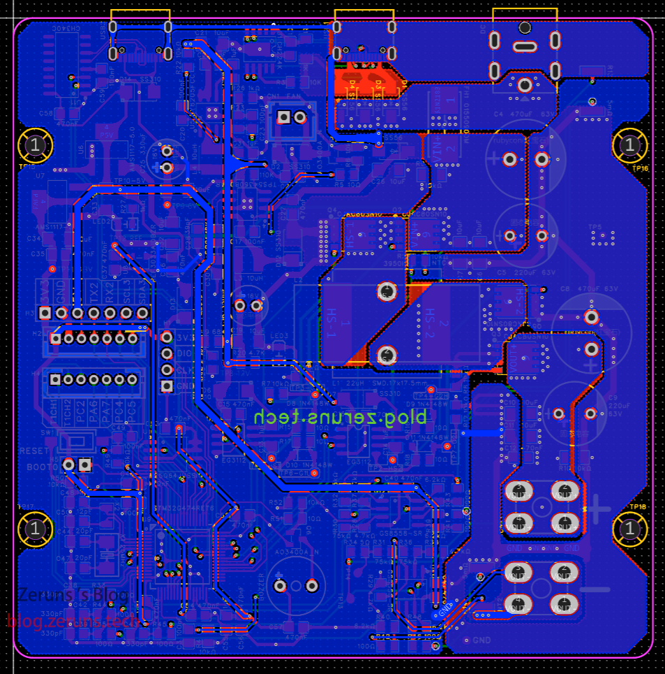
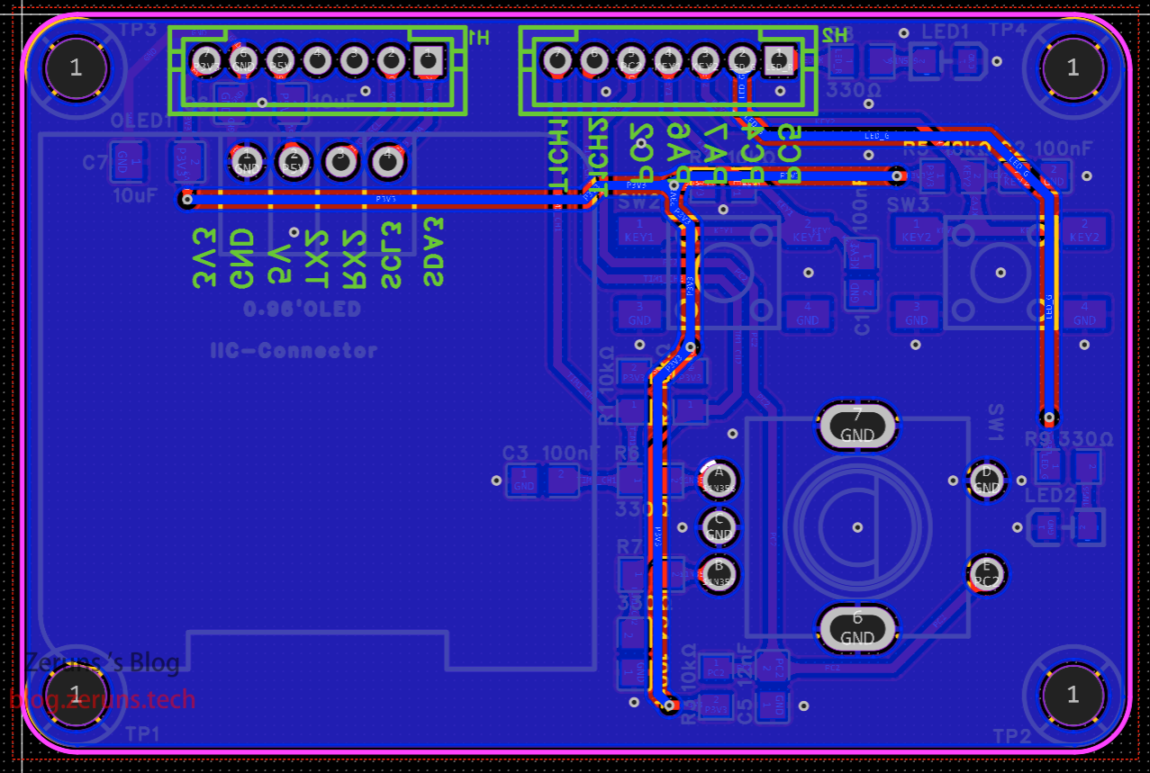
PCB Screenshots
Power Board Top Layer
Power Board GND Layer
Power Board Inner Layer 2
Power Board Bottom Layer
Panel Top Layer
Panel Bottom Layer
Instructions for Use
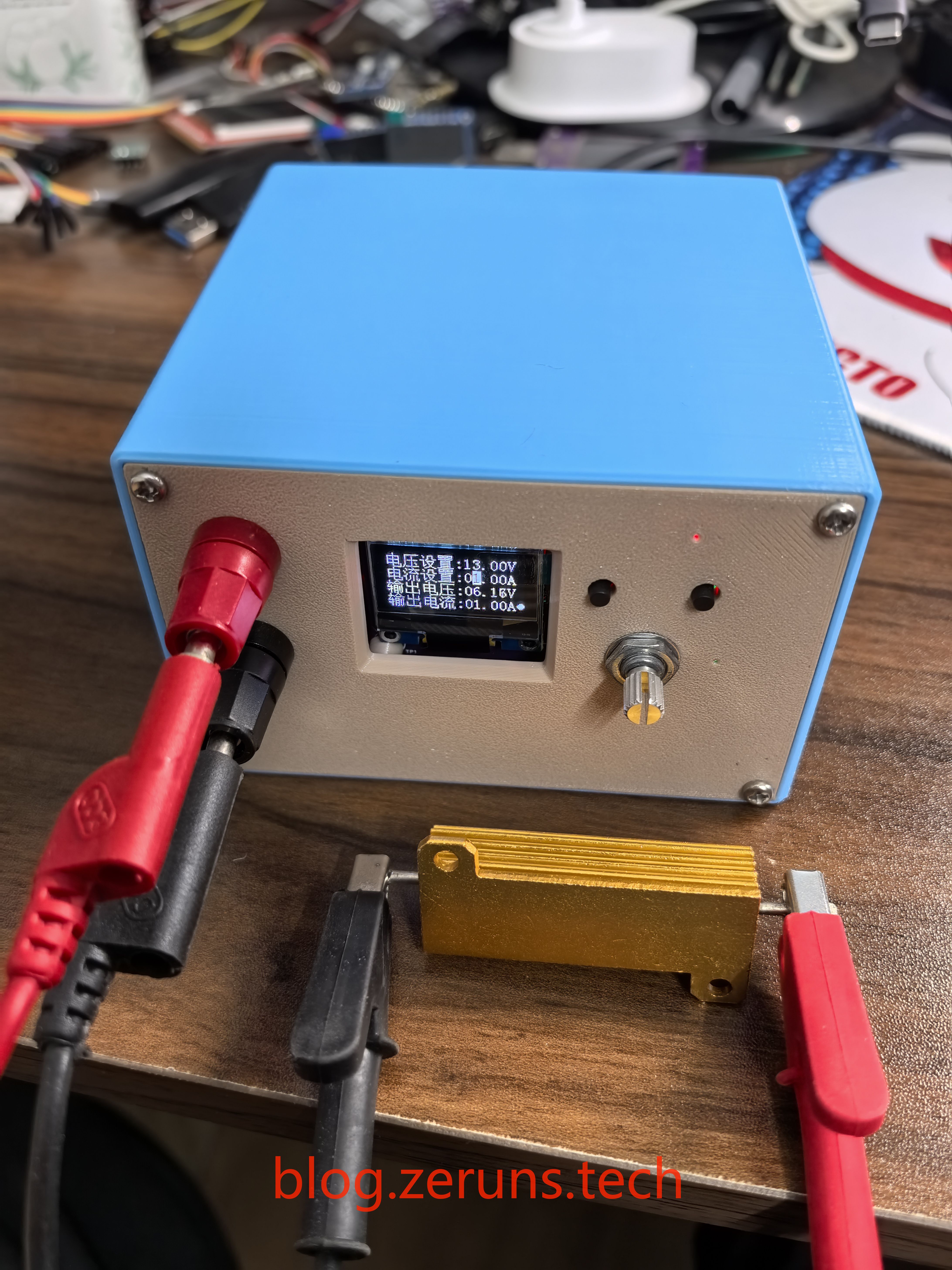
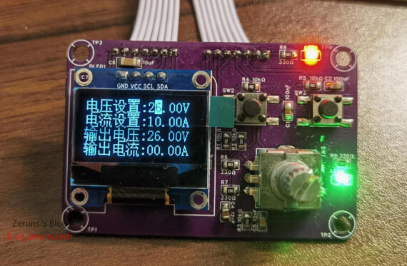
You can set the output voltage and current values through buttons and a rotary encoder. As shown in the figure below, the inverted display value is the current bit to be set. By rotating the encoder, you can increase or decrease the value. Pressing the encoder switches to the next bit for setting. The SW2 button can be used to switch between the items to be set. The set data will be automatically saved to the Flash storage chip, and the data will be read from the storage chip when powered on next time.
The SW3 button turns the power output on/off.
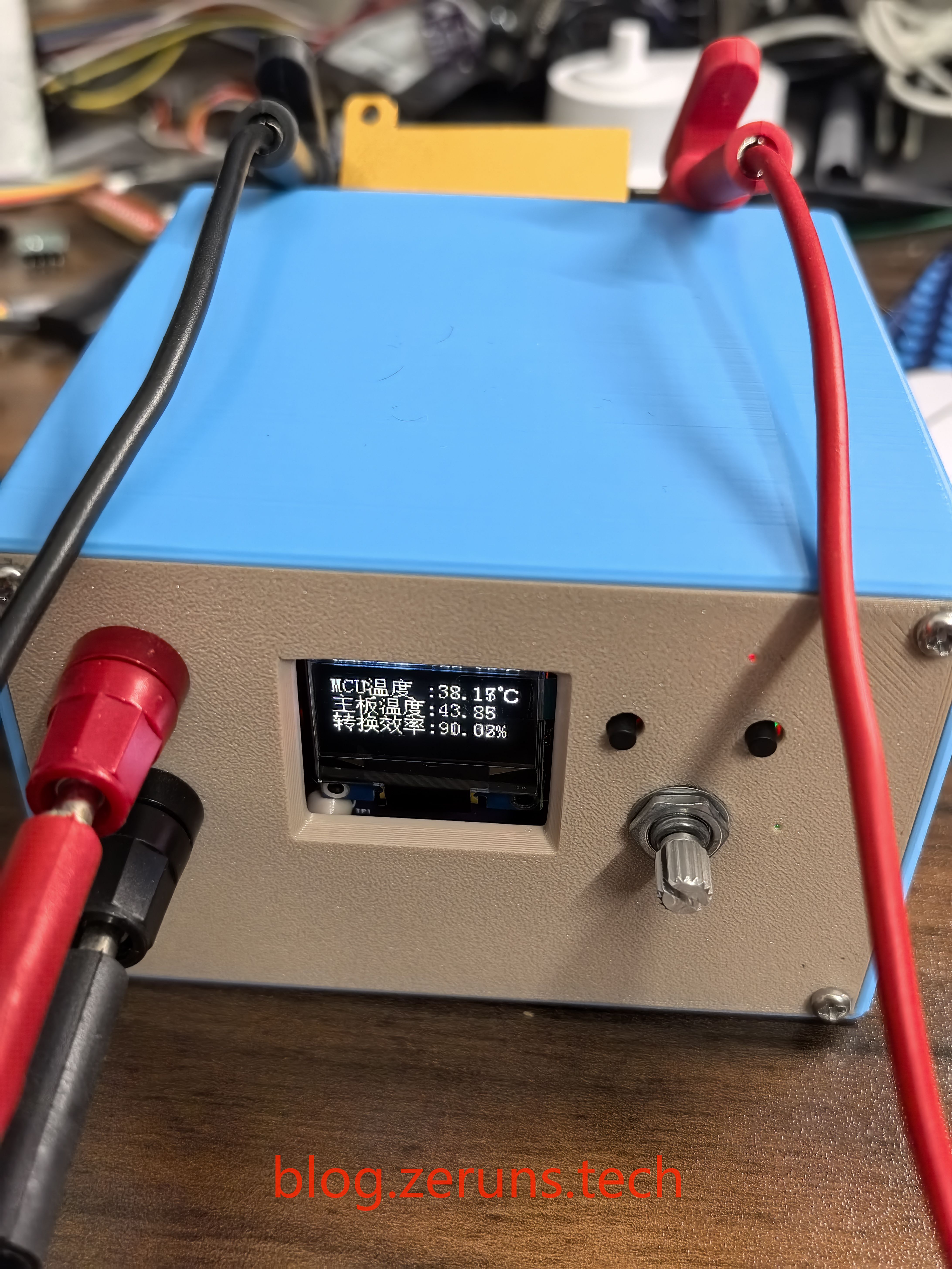
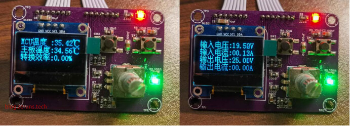
You can switch to the data display page to view the current input/output voltage and current of the power supply, as well as information such as the motherboard temperature and MCU temperature, as shown in the figure below.
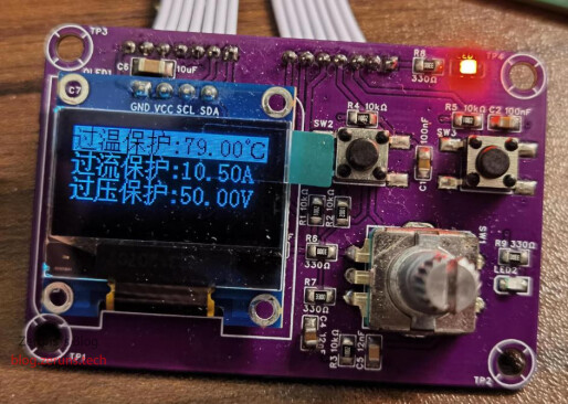
You can switch to the settings page to set the thresholds for overheat/overcurrent/overvoltage protection, as shown in the figure below. The set data will be automatically saved to the Flash storage chip, and the data will be read from the storage chip when powered on next time.
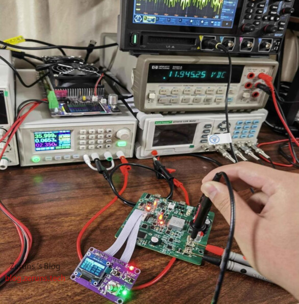
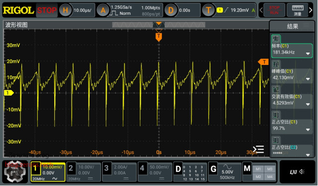
Ripple Test
An electronic load and oscilloscope are used to test the power supply output performance and output ripple, as shown in the figure below. At 36V input and 12V 2A output, the ripple peak-to-peak value is measured to be approximately 42mV, as shown in the figure below.
Conversion Efficiency Test
The power conversion efficiency at 20V input and 12V 10A output is tested to be 92%, as shown in the figure below.
The following table shows the conversion efficiency at various different input and output voltages, with the highest efficiency being 94.3%.
| Input Voltage (V) | Input Current (A) | Input Power (W) | Output Voltage (V) | Output Current (A) | Output Power (W) | Conversion Efficiency (%) |
|---|---|---|---|---|---|---|
| 20.003 | 4.035 | 80.712 | 15.010 | 5.000 | 75.050 | 92.985 |
| 47.999 | 5.335 | 256.075 | 24.040 | 9.900 | 237.996 | 92.940 |
| 48.000 | 7.875 | 378.000 | 36.020 | 9.900 | 356.598 | 94.338 |
| 48.000 | 9.860 | 473.280 | 45.030 | 9.900 | 445.797 | 94.193 |
| 23.998 | 8.835 | 212.022 | 48.070 | 4.000 | 192.280 | 90.689 |
| 23.998 | 9.830 | 235.900 | 35.998 | 6.001 | 216.024 | 91.574 |
| 12.099 | 9.166 | 110.899 | 24.070 | 4.000 | 96.280 | 86.817 |
| 20.008 | 2.645 | 52.921 | 4.970 | 9.000 | 44.730 | 84.522 |
| 20.008 | 10.550 | 211.084 | 24.030 | 8.000 | 192.240 | 91.073 |
| 36.000 | 6.418 | 231.048 | 24.010 | 9.000 | 216.090 | 93.526 |
| 36.000 | 10.540 | 379.440 | 35.950 | 9.800 | 352.310 | 92.850 |
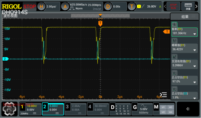
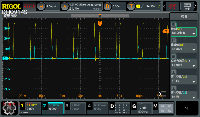
MOS Gate Waveform
Testing the gate waveforms of each MOS at 20V input and 24V output.
BUCK circuit upper and lower tube voltage waveform relative to ground:
BOOST circuit upper and lower tube voltage waveform relative to ground:
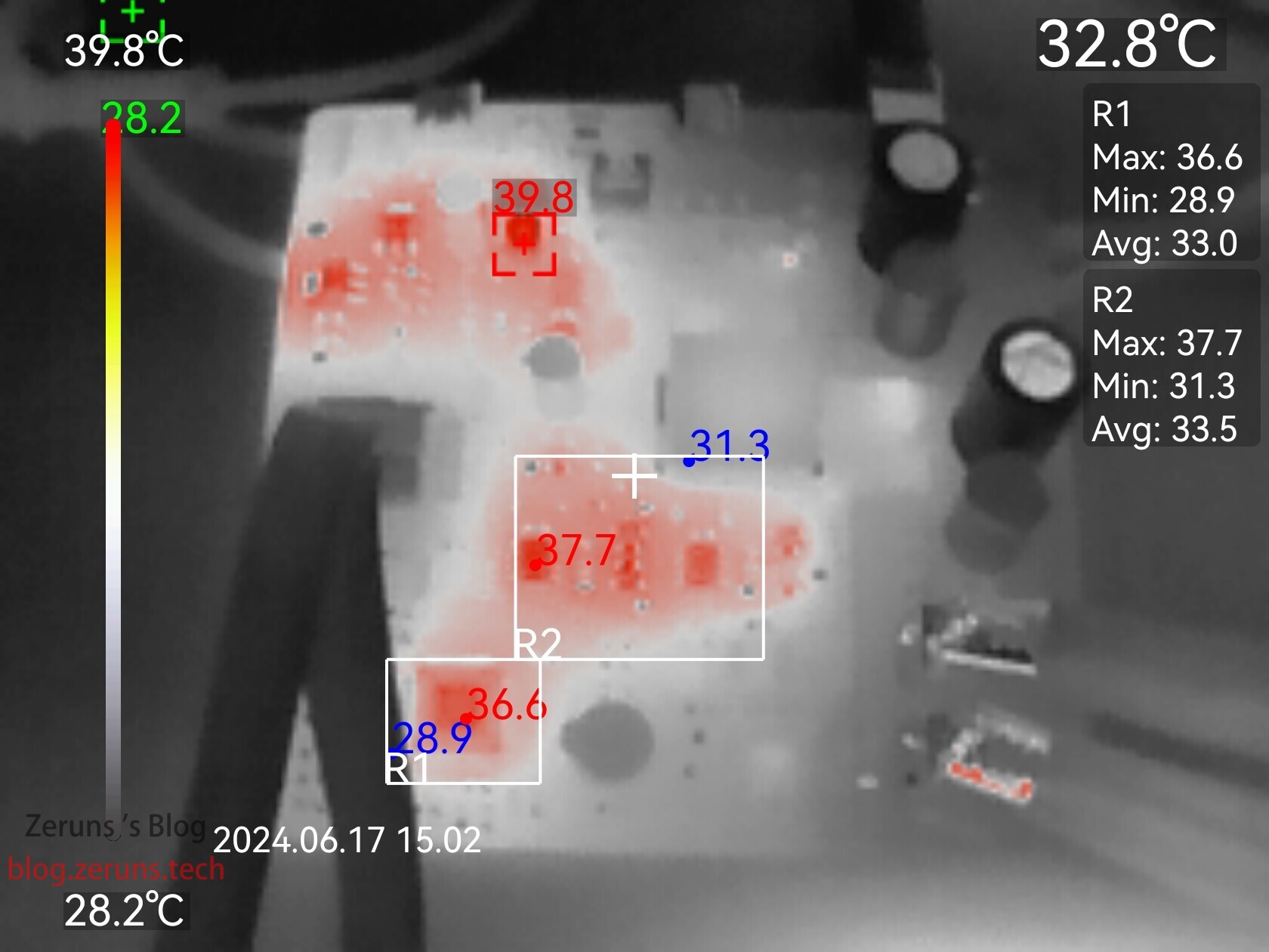
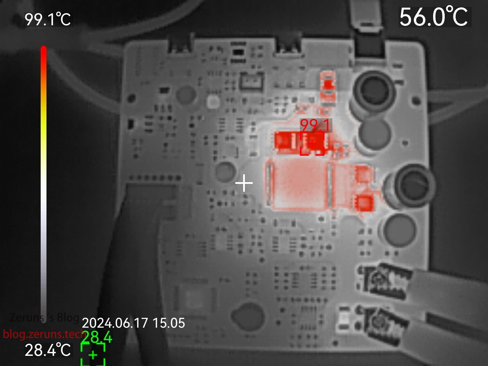
Heat Generation Test
Thermal image at no load:
Thermal image after outputting 10A current for 10 minutes, with MOS temperature around 100°C:
Unboxing review of Uni-Trend UTi261M thermal imaging camera: https://blog.zeruns.com/archives/798.html
Component Purchase Address
Most of the components used in this project can be purchased at the following addresses:- 0805 Resistor and Capacitor Sample Book: https://s.click.taobao.com/begdskt
- STM32G474RE Chip: https://s.click.taobao.com/C5yYWlt
- CH224K Chip: https://s.click.taobao.com/4t4bskt
- CJAC80SN10 MOS Transistor: https://s.click.taobao.com/aPsWWlt
- EG3112 Chip: https://s.click.taobao.com/1k9Zskt
- 220μF 63V Solid State Capacitor: https://s.click.taobao.com/n60Yskt
- 470μF 63V Ruby Capacitor: https://s.click.taobao.com/WTRUWlt
- GS8558 Op-Amp: https://s.click.taobao.com/usSVskt
- TPS54360 Chip: https://s.click.taobao.com/r6lSWlt
- SY8205 Chip: https://s.click.taobao.com/GxMUskt- AMS1117 Chip: https://s.click.taobao.com/mxASWlt
- REF3033 Reference Chip: https://s.click.taobao.com/eOcTskt
- W25Q64JVSSIQ Chip: https://s.click.taobao.com/QX7Tskt
- CH340C Chip: https://s.click.taobao.com/QYRQWlt
- 3.3V Active Buzzer: https://s.click.taobao.com/sovPWlt
- Type-C Female Connector 16P: https://s.click.taobao.com/vjLRskt
It is recommended to purchase components from Lichuang EDA: https://activity.szlcsc.com/invite/D03E5B9CEAAE70A4.html
Click “Order Now at Lichuang Mall” in the BOM table on the Lichuang Open Source link to import all required components into your shopping cart with one click.
Resource Download Links
The links below contain: Lichuang EDA projects, schematic PDF files, datasheets for each chip, source code project archives, and some reference program code.
123 Cloud Drive Unlimited Speed Download: https://www.123pan.com/ps/2Y9Djv-8yevH.html
Baidu Netdisk Download: https://url.zeruns.com/MW2d1
Project Program Gitee Open Source Address: https://gitee.com/zeruns/STM32-Buck-Boost
Project Program GitHub Open Source Address: https://github.com/zeruns/Synchronous-Rectification-Buck-Boost-Digital-Power-Supply-Based-on-STM32
Please give a Star and a Like.
Known Issues
- The SY8205 chip in the auxiliary power supply enters PFM mode under light load, resulting in lower frequency and slight noise.
- The PID control program for constant current mode is not well written; constant current is only stable under pure resistive loads. (Constant voltage mode has no issues)
Other Open Source Projects Recommended
- Developed a three-phase power meter open source project that can conveniently monitor home electricity usage: https://blog.zeruns.com/archives/771.html
- LVGL project template based on STM32F407 (MSP3526 screen), including FreeRTOS and bare metal versions: https://blog.zeruns.com/archives/788.html
- Qinheng CH32V307VCT6 minimum system board open source: https://blog.zeruns.com/archives/726.html
- LM25118 automatic buck-boost adjustable DCDC power module: https://blog.zeruns.com/archives/727.html
- EG1164 high-power synchronous rectification boost module open source, maximum efficiency 97%: https://blog.zeruns.com/archives/730.html
- 4G environmental monitoring node based on Hezhou Air700E (temperature, humidity, atmospheric pressure data, etc.), uploaded to Alibaba Cloud IoT platform via MQTT: https://blog.zeruns.com/archives/747.html
- Intelligent electronic load open source based on HT32F52352, Holtek Cup competition work: https://blog.zeruns.com/archives/784.html
Recommended Reading
- High Cost-Performance and Cheap VPS/Cloud Server Recommendations: https://blog.zeruns.com/archives/383.html
- Minecraft Server Setup Tutorial: https://blog.zeruns.com/tag/mc/
- Build a Blog Website Without Code! Super Detailed Personal Blog Setup Tutorial: https://blog.zeruns.com/archives/783.html
- Intranet Penetration Server Setup Tutorial, NPS Setup and Usage Guide: https://blog.zeruns.com/archives/741.html
- Rainyun Ningbo 8272CL High Bandwidth DDoS Protection Cloud Server Performance Review, up to 500Mbps Bandwidth and 1TB Cloud Storage: https://blog.zeruns.com/archives/789.html
- Douyin Mall 2.6 Yuan 120W Charger Test and Teardown: https://blog.zeruns.com/archives/786.html