DJI Mini 2 Drone: Simple Disassembly and Analysis
Four years ago, I purchased a DJI Mini 2 drone, and recently I noticed extremely weak 5.8GHz video transmission signal. After searching online, I found this issue is suspected to be caused by a faulty 5.8GHz RF power amplifier chip—a known common failure. Since the warranty had expired, I decided to attempt a DIY replacement.
Note: Some chip interpretations in this article include AI-generated content.
DJI Mavic Mini 2 Drone: Simple Unboxing Review: https://blog.zeruns.com/archives/650.html
Other Disassembly Articles
- GL-RM1PE: Simple Unboxing and Disassembly: https://blog.zeruns.com/archives/900.html
- ZGRL-80 Photography Light Disassembly and Circuit Analysis: https://blog.zeruns.com/archives/882.html
- ZTE F7015TV3 2.5G Optical Modem Disassembly: https://blog.zeruns.com/archives/797.html
- Radian D1500 UPS (Uninterruptible Power Supply) Disassembly Analysis: https://blog.zeruns.com/archives/792.html
- Testing and Disassembly of a 2.6 RMB 120W Charger from Douyin Mall: https://blog.zeruns.com/archives/786.html
- Apple Mac Mini M4 Mini Desktop: Simple Review and Disassembly: https://blog.zeruns.com/archives/851.html
Disassembly
Remove the four cross-head screws around the bottom of the drone.

Remove the battery and pry open the housing clips on both sides of the battery compartment.
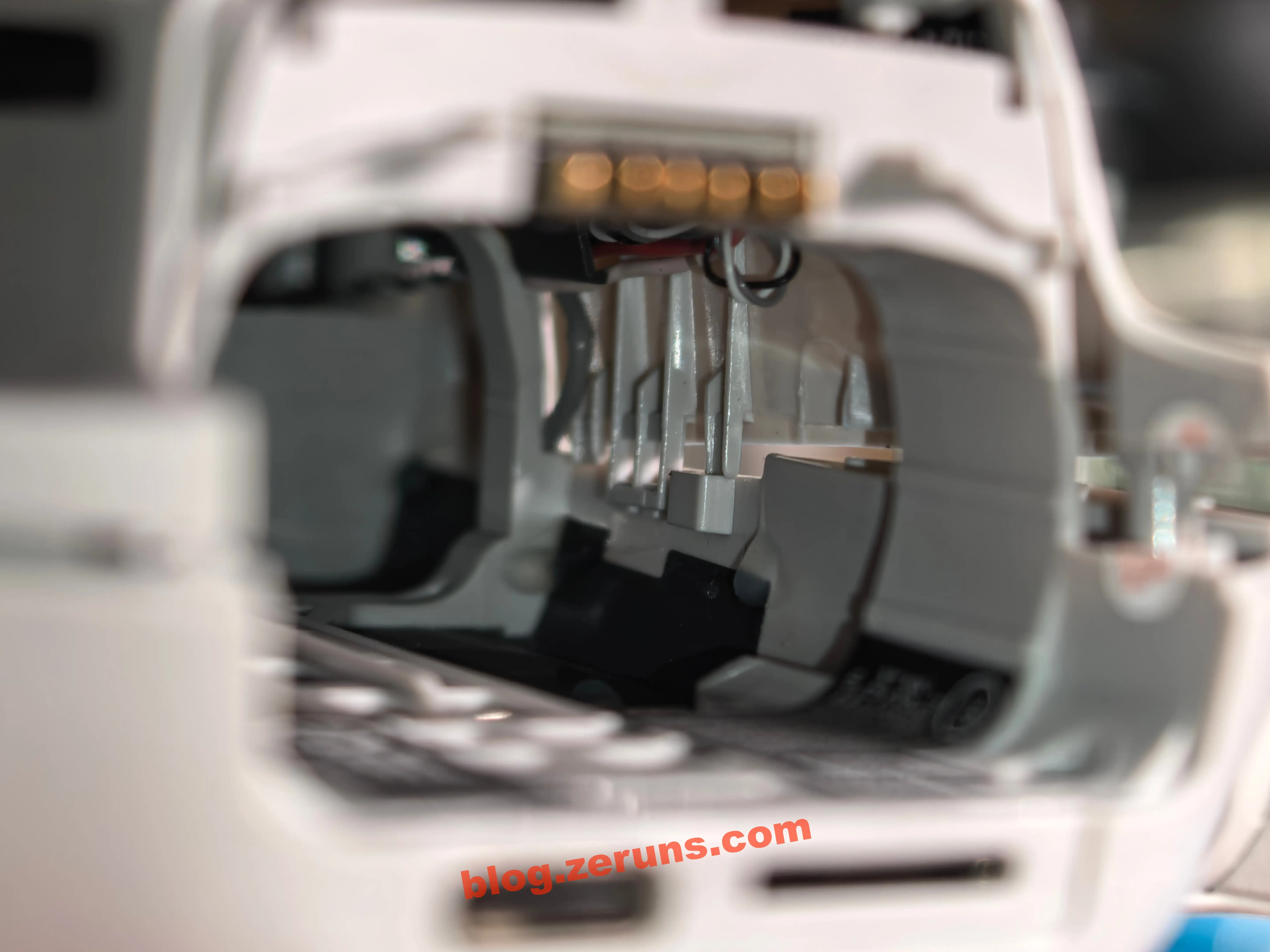
The upper housing cover can now be removed. In the center, you’ll see the GPS ceramic antenna.
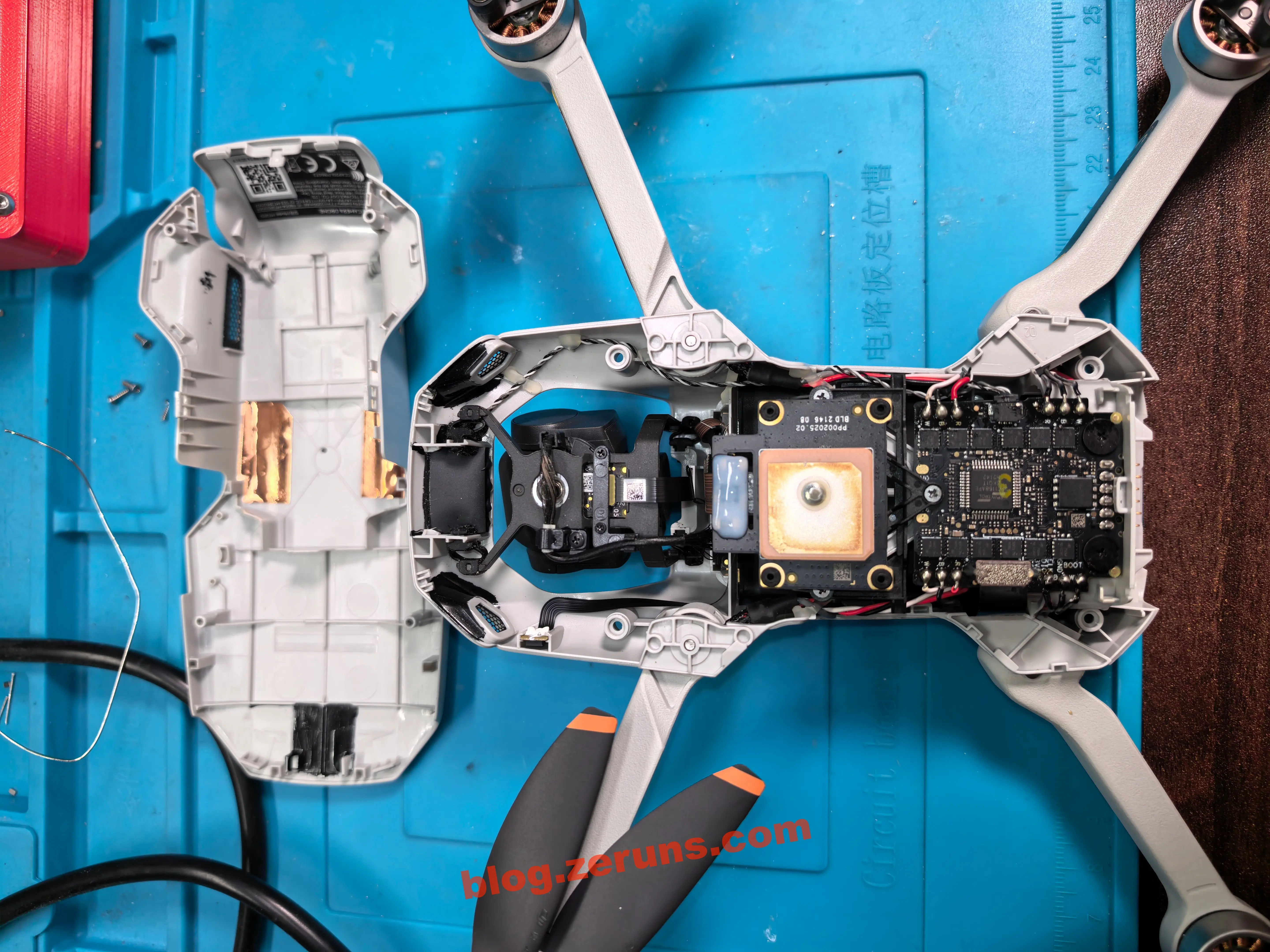
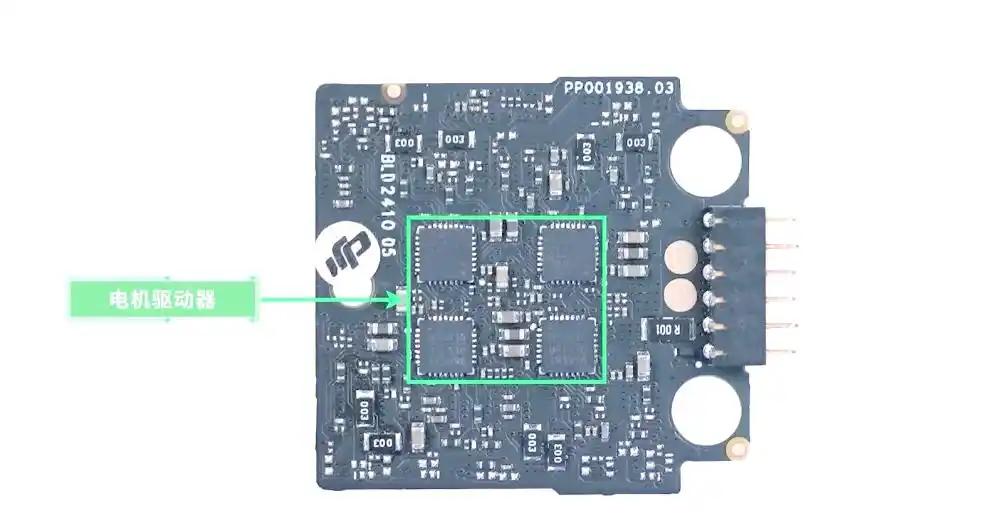
Beneath the GPS antenna lies the three-phase sensorless BLDC (Brushless DC Motor) driver board. The central chip on the board is labeled SPC1168APE48, a highly integrated system-on-chip (SoC) microcontroller from SpinTrol. It is likely used for motor control, driving the surrounding MOSFETs.
The SPC1168 features a 32-bit high-performance ARM Cortex-M4 core with a software-programmable clock frequency up to 200 MHz, 64KB SRAM, 128KB embedded FLASH, and abundant enhanced I/O and peripheral resources. It includes a 14-bit ADC, three programmable gain amplifiers, six enhanced PWM modules, three general-purpose 32-bit timers, and communication interfaces such as UART, I2C, and SPI—making it an ideal platform for motor control applications. Additionally, it incorporates two innovative technologies: multi-zone security protection to enhance code security, and FPGA-like flexible I/O technology that allows I/O pins to be reconfigured for different peripherals, supporting diverse application needs at lower cost.

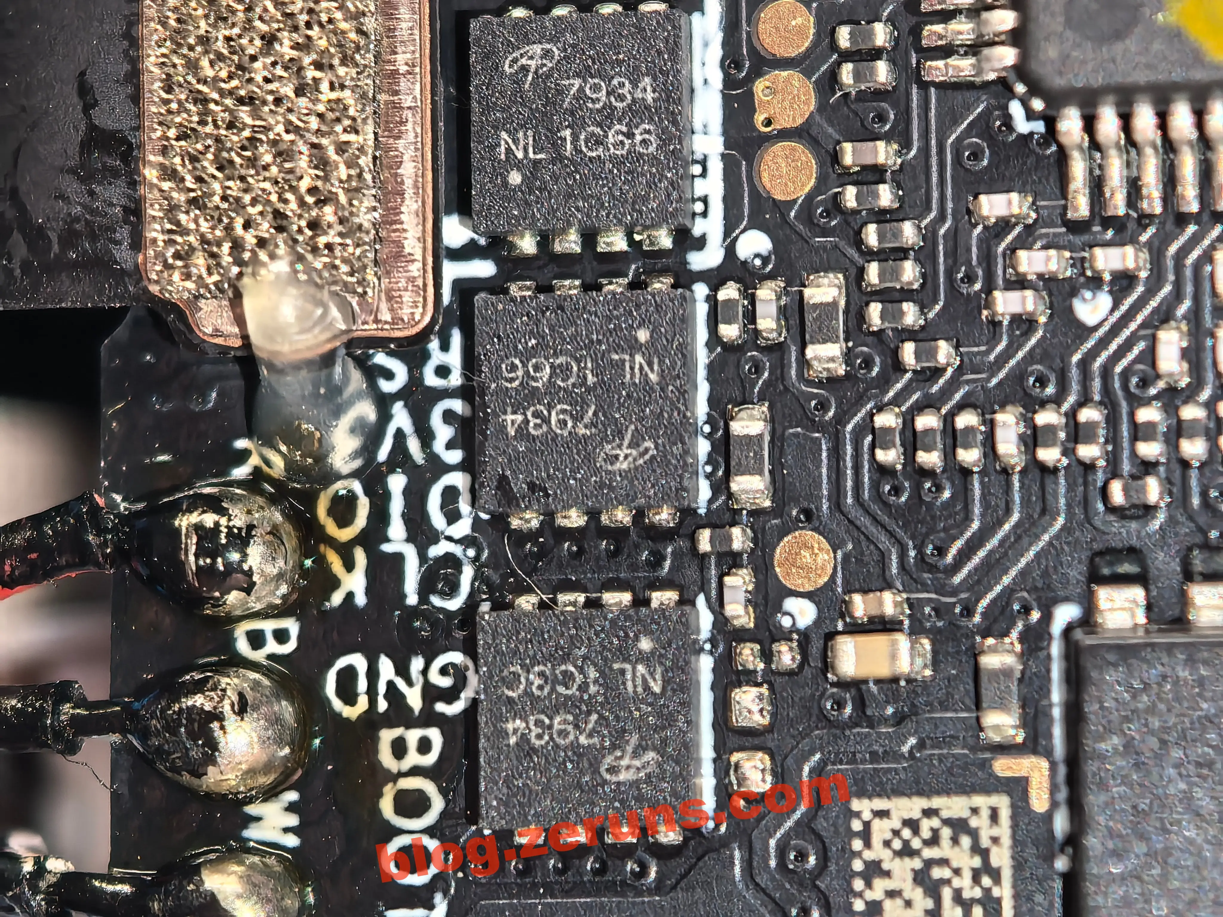
Around the motor driver board are four groups of MOSFET chips (three per group), each corresponding to one of the four propeller motors. All MOSFETs are AON7934, dual N-channel MOSFETs from Alpha and Omega Semiconductor (AOS), with two NMOS transistors integrated into a single half-bridge per chip.
Key Chip Specifications:
- Electrical Performance:
- Drain-Source Voltage (Vds): 30V
- Continuous Drain Current (Id): 16A/18A (per channel)
- On-Resistance (Rds(on)): Minimum 10.2 mΩ @ 16A, 10V
- Input Capacitance (Ciss): 485 pF
- Package and Reliability: DFN-8 (3x3) package, operating temperature range: -55°C to 150°C, meeting reliability requirements for outdoor drone environments.
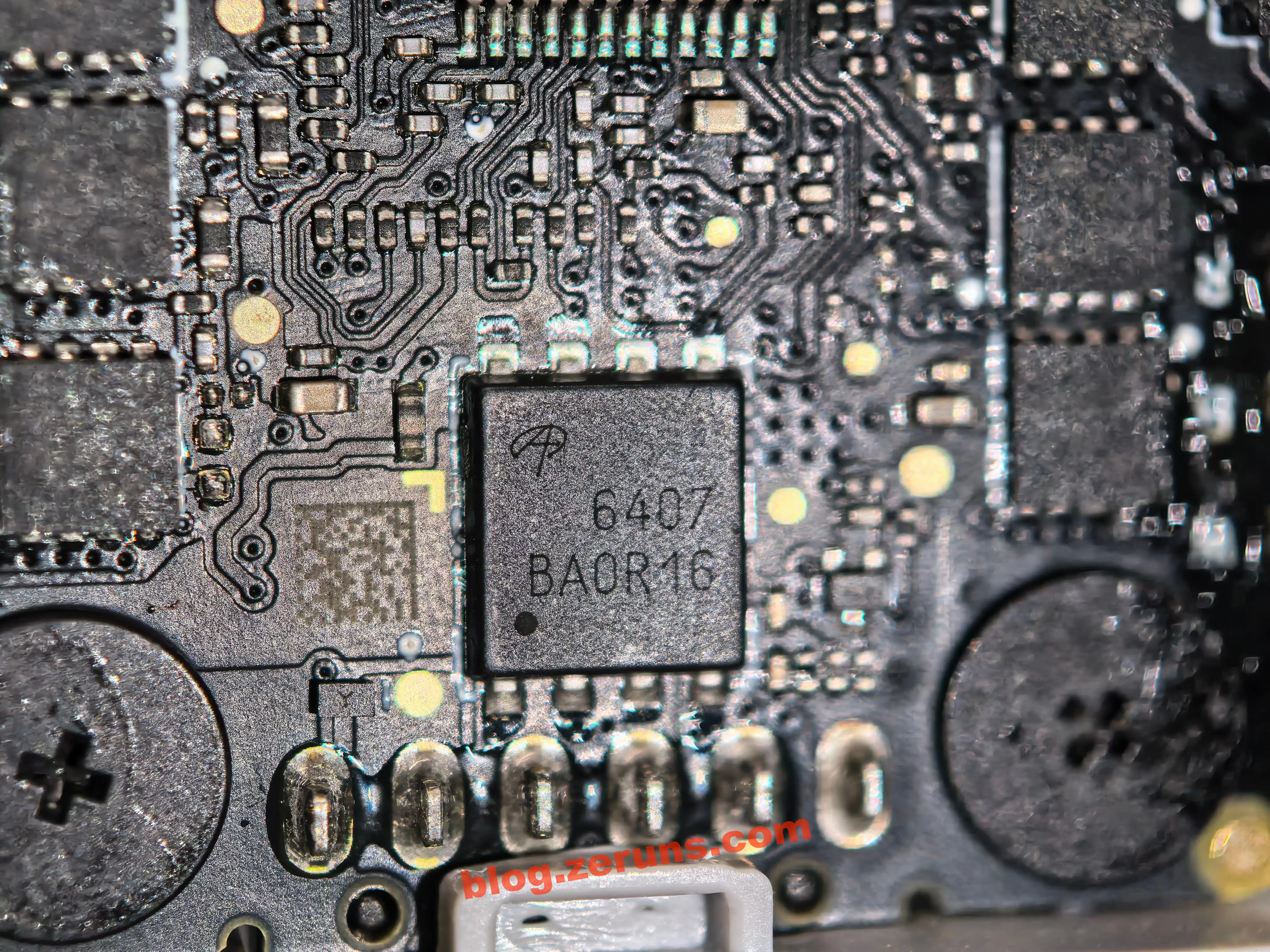
Above the battery connector is a chip labeled AON6407, a P-channel power MOSFET from AOS.
Key Specifications and Features:
- Electrical Performance: Drain-Source Voltage (Vds): -30V, Continuous Drain Current (Id): -85A, On-Resistance (Rds(on)): 4.5 mΩ
- Package Design: PDFN-8 (5.8x4.9) package
Function Analysis:
The AON6407 serves as the power switch for the battery circuit, positioned above the battery connector to perform the following critical functions:
- Power On/Off Control: Manages power flow between the battery and the drone’s main circuit, enabling precise startup and shutdown.
- Efficient Power Delivery: With its low on-resistance (4.5 mΩ), it minimizes power loss during battery discharge, improving energy efficiency and indirectly extending flight time.
- Circuit Protection: Rapidly shuts down the circuit under abnormal conditions such as overcurrent or overvoltage, preventing damage to the battery or downstream components and ensuring power system reliability.
In short, it acts as the “power gate” between the battery and the drone’s core circuitry—ensuring efficient energy delivery while safeguarding the power system.
On the back of the motor driver board are four MP6530 chips from MPS (Monolithic Power Systems), gate driver ICs specifically designed for three-phase brushless DC motor drivers. Each can drive a half-bridge formed by six N-channel power MOSFETs and supports voltages up to 60V.
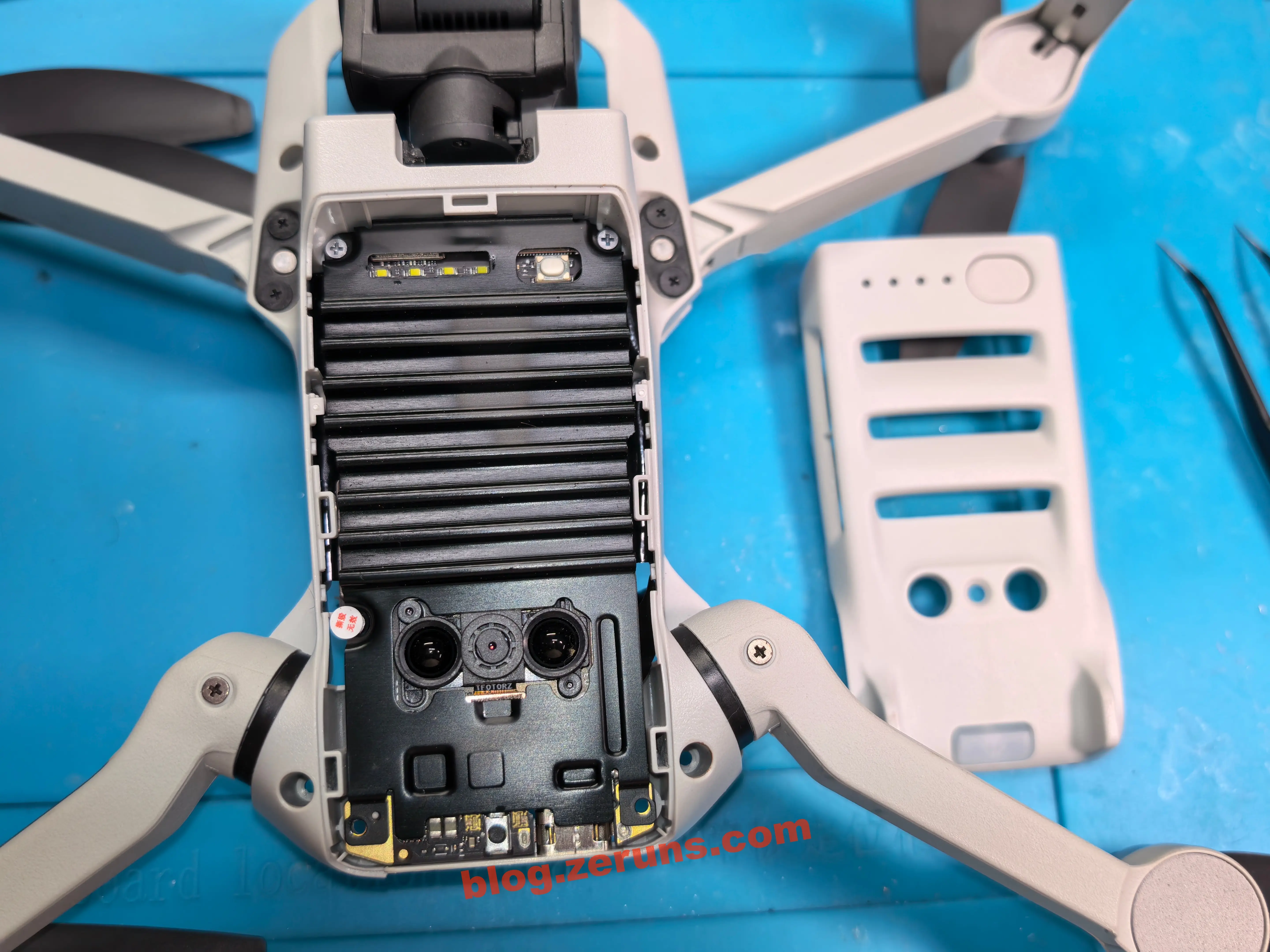
Remove the two cross-head screws beneath the battery compartment to detach the bottom cover.
The first thing visible is a large black aluminum heatsink, beneath which lie the downward-facing camera and infrared distance sensor module.
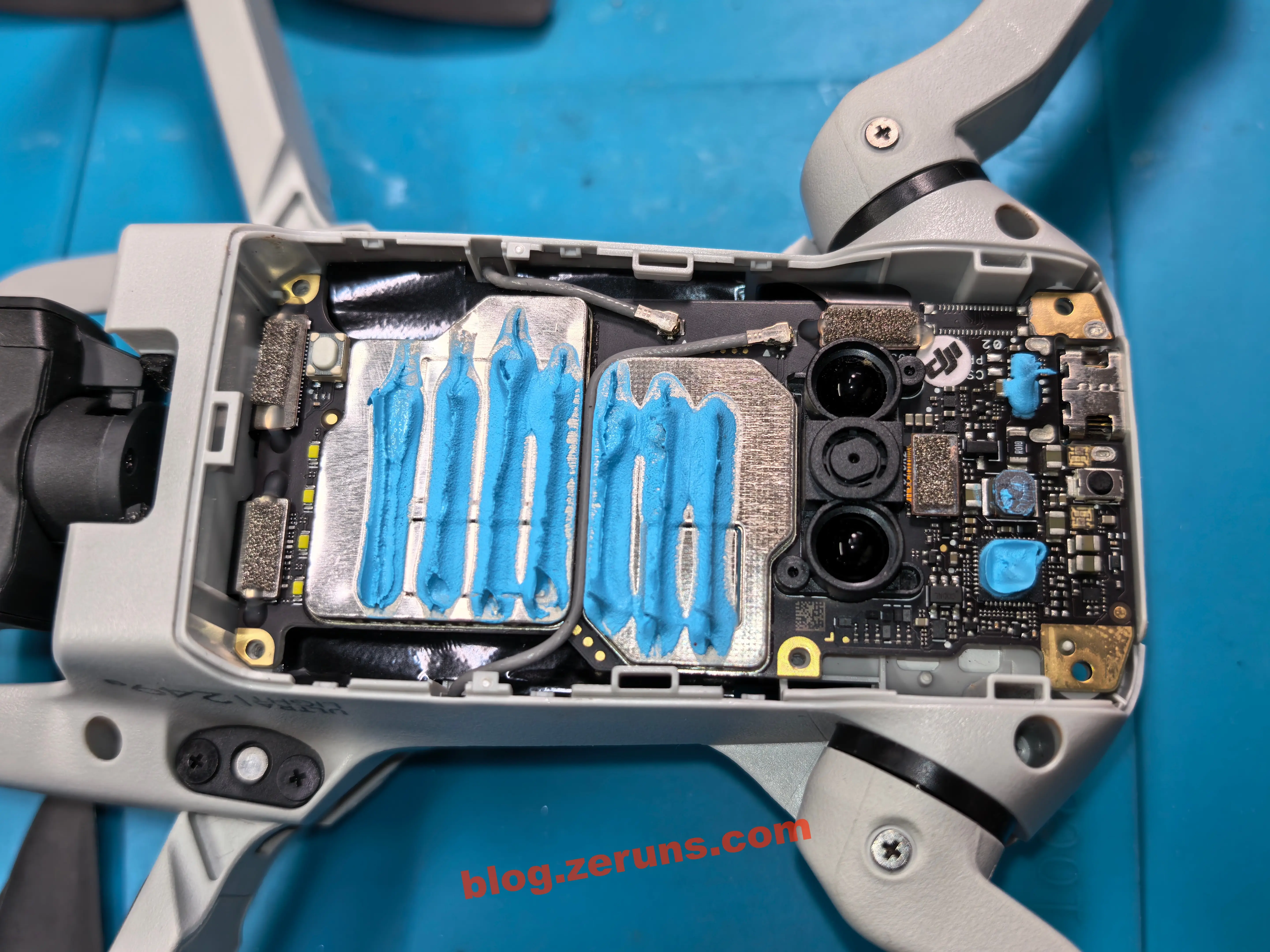
After removing the heatsink, you’ll notice blue thermal paste applied to the shield and some chips.
Remove the mainboard. On its reverse side are the Type-C charging port and TF card slot.

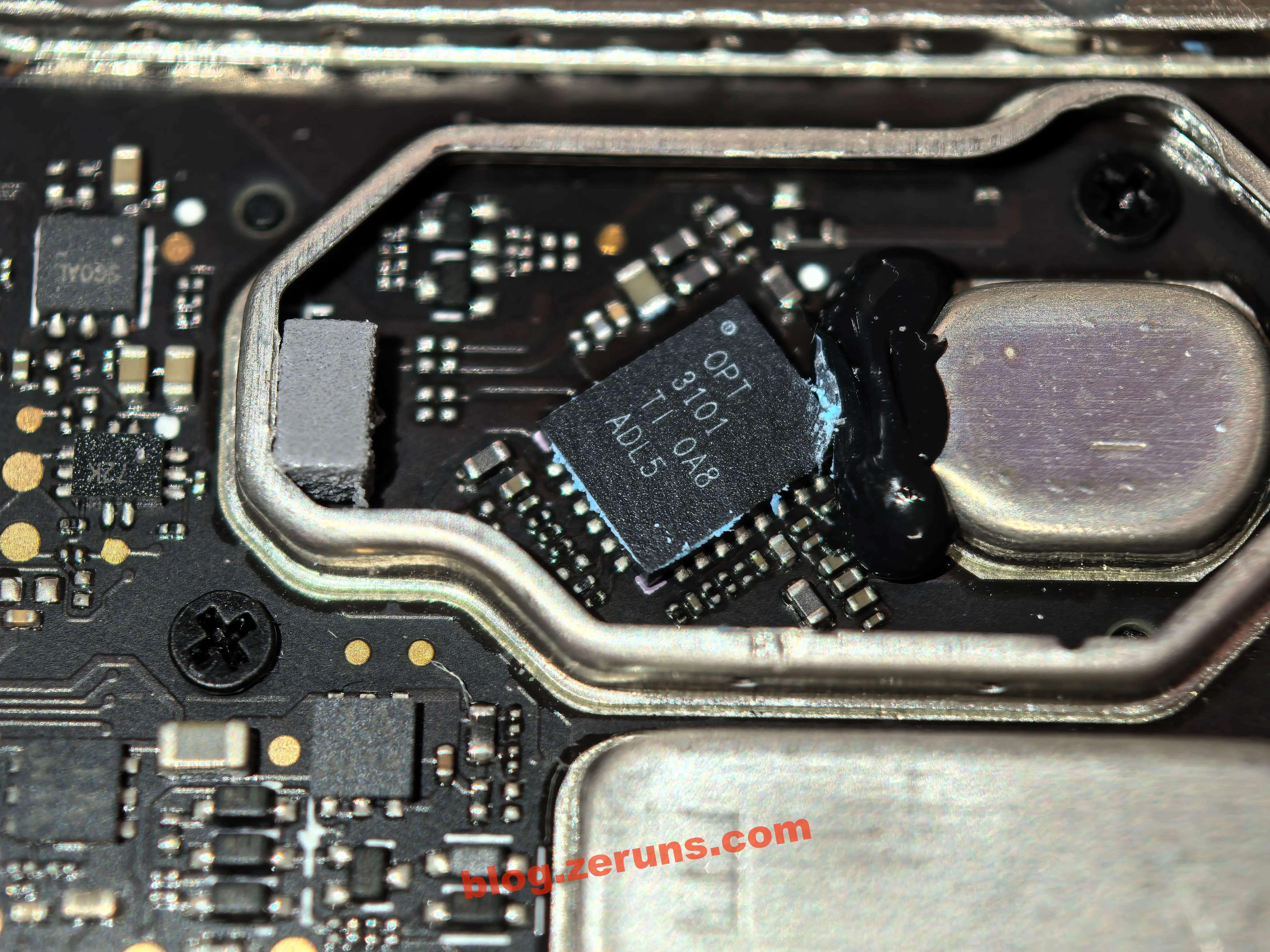
Lift the shield beneath the TF card slot (the opposite side of the PCB here houses the downward camera module). Inside is a Texas Instruments (TI) OPT3101 chip.
Core Attributes and Functions:
- Technology Type: Time-of-Flight (ToF) based long-range proximity and distance sensor analog front-end (AFE).
- Performance Highlights:
- Range: Accurate up to 15 meters, supports 16-bit distance output with 3mm resolution;
- Environmental Adaptability: Excellent ambient light rejection, operates under 130 klx full sunlight;
- Integration: Built-in ADC, timing sequencer, digital processing engine, and lighting driver supporting three transmitter channels.
Role in the Device:
As the ToF sensing core, it enables:
- Precise Distance Measurement: Provides real-time distance data for flight control and obstacle avoidance;
- Environmental Awareness: Detects distance and position of surrounding obstacles via multi-zone sensing, enhancing intelligent interaction and safety;
- Interference Immunity: Unaffected by object reflectivity, delivers stable depth data even under complex lighting conditions.
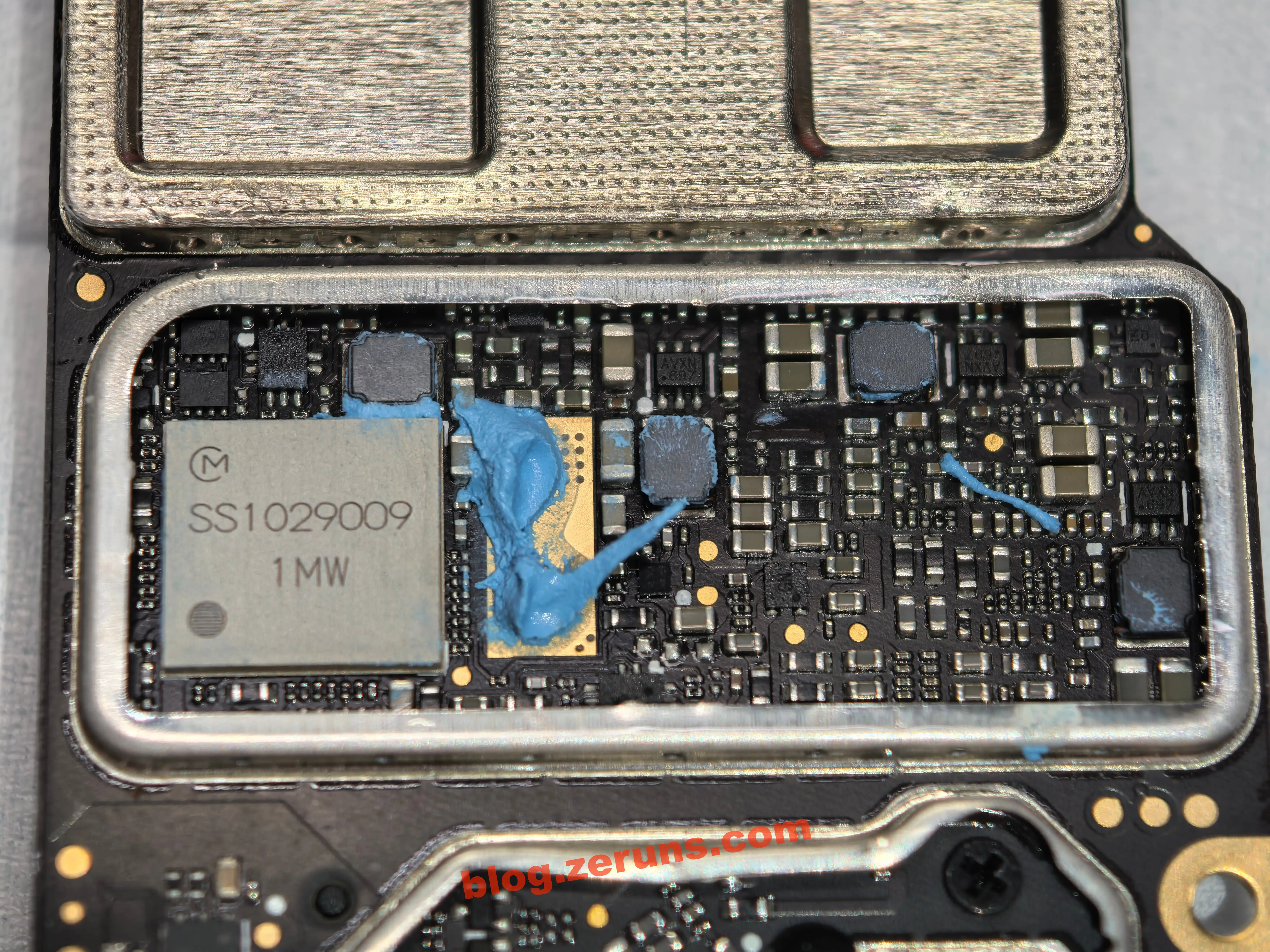
Inside the central shield is a muRata (Murata) chip labeled SS1029009, suspected to be the modulator/demodulator for the drone’s video transmission signal.
Inside the largest shield are three major chips: MIMXRT1064, TC58NVG1S3H, and NT5CB128M16JR-FL.
1. i.MX RT1064 (MIMXRT1064)
- Brand and Positioning: NXP’s high-performance crossover processor from the i.MX RT series.
- Core Specifications:
- Core: Cortex-M7, up to 600 MHz clock speed.
- Memory: Supports external DDR and Flash expansion, enabling high-speed data processing.
- Function: Serves as the main controller of the DJI Mini 2, handling flight control, sensor fusion, and image preprocessing—essentially the drone’s “brain.”
2. TC58NVG1S3H (Toshiba Flash Chip)
- Brand and Positioning: Toshiba SLC NAND flash chip.
- Core Specifications:
- Capacity: 2 Gbit (256 MB), industrial-grade storage.
- Features: High-speed read/write, power-loss data protection.
- Function: Stores firmware, flight logs, and calibration parameters, ensuring system stability during boot and operation.
3. NT5CB128M16JR-FL (Nanya DDR Memory)
- Brand and Positioning: Nanya DDR3 memory chip.
- Core Specifications:
- Capacity: 128M×16bit (2 Gbit = 256 MB), operating voltage 1.5V.
- Data Rate: Up to 2133 MT/s (equivalent to DDR3-2133), clock frequency 1066 MHz.
- Performance: High bandwidth to meet the main controller’s demands.
- Function: Acts as system RAM, providing temporary data storage for the i.MX RT1064 to ensure smooth execution of flight control algorithms and real-time image processing.

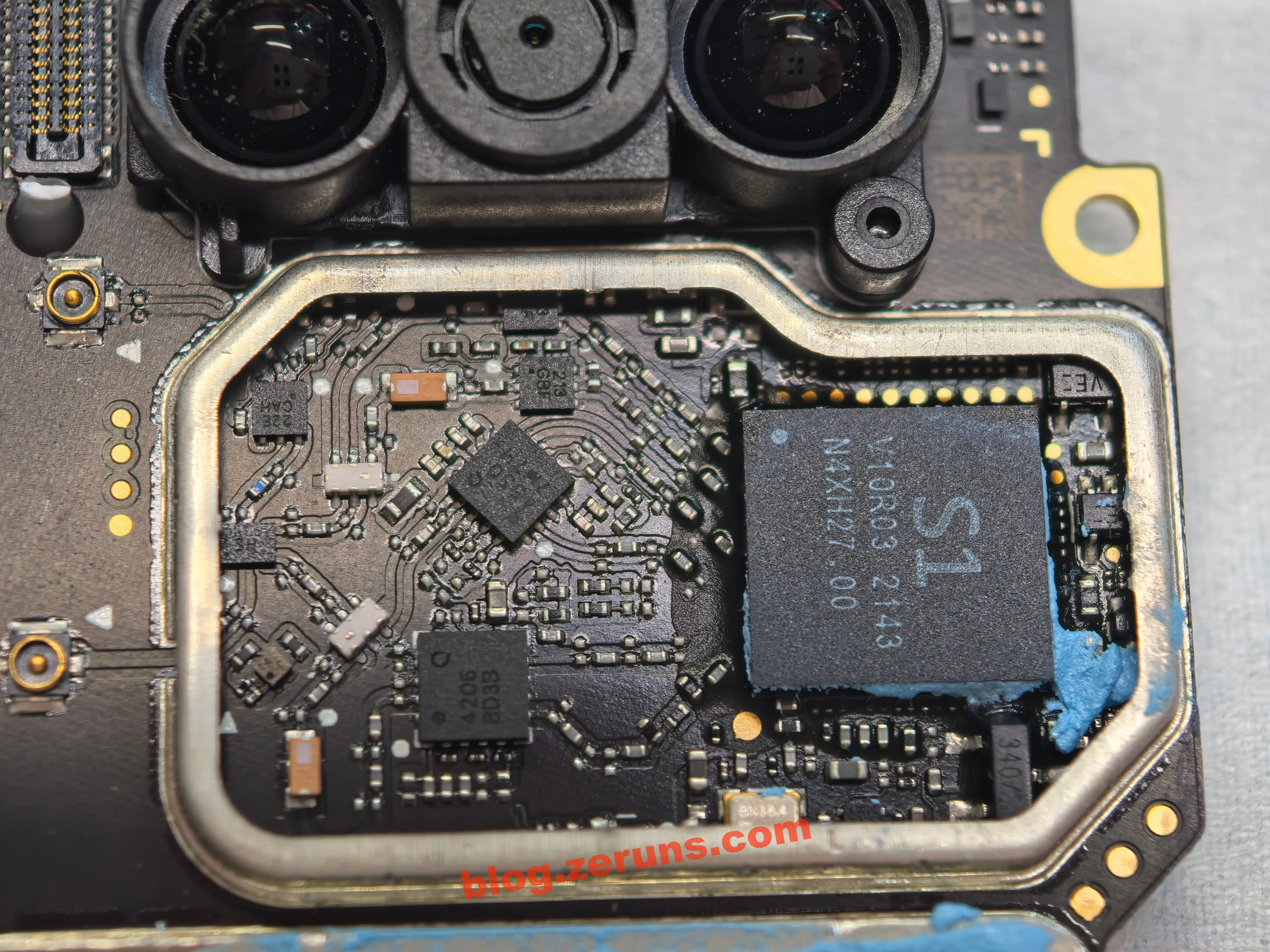
Beneath the downward camera module’s shield are three main chips: S1 V10R03, 4205, and 4550.
1. S1 V10R03 Chip
- Type: Customized video transmission communication chip (part of DJI’s OcuSync S1 series, codenamed “Sparrow 1”).
- Function: Core of the drone’s video transmission system, responsible for RF modulation/demodulation, data transmission, and encryption. It is the key component enabling low-latency, high-stability video transmission. It handles only RF communication; video encoding is managed by other chips, making it function more like a “modem” in entry-level models like the Mini series.
- Characteristics: Supports up to 20 MHz bandwidth, uses a proprietary architecture optimized for DJI’s wireless link, exclusive to DJI ecosystem products—part of its technological moat.
2. 4205 Chip
- Type: 2.4 GHz RF power amplifier (likely a variant of QPF4206, with simplified silkscreen markings).
- Function: Amplifies the 2.4 GHz wireless signal to extend transmission range and improve interference resistance. The 2.4 GHz band is used by the Mini 2 for long-range communication (e.g., open-area flights). This chip is critical to maintaining performance on this band.
- Characteristics: Operates at 2.4 GHz with high power efficiency, boosting transmit power to regulatory limits while minimizing power consumption to suit drone battery life.
3. 4550 Chip
- Type: 5.8 GHz RF power amplifier (model QPF4550).
- Function: Amplifies the 5.8 GHz wireless signal. This band offers wider bandwidth for HD video transmission but has weaker penetration. This chip boosts the 5.8 GHz signal strength to ensure stable HD transmission in short-range, low-interference environments (e.g., urban close-range shooting with low latency).
- Characteristics: Optimized for 5.8 GHz, high power efficiency, maintains signal quality during high-bandwidth transmission—key hardware for the Mini 2’s “low-latency video transmission.”
These three chips work together to form the Mini 2’s wireless communication system: S1 handles signal “encoding and transmission management,” while 4205 and 4550 amplify the 2.4 GHz and 5.8 GHz signals respectively, delivering long-range, low-latency video transmission.
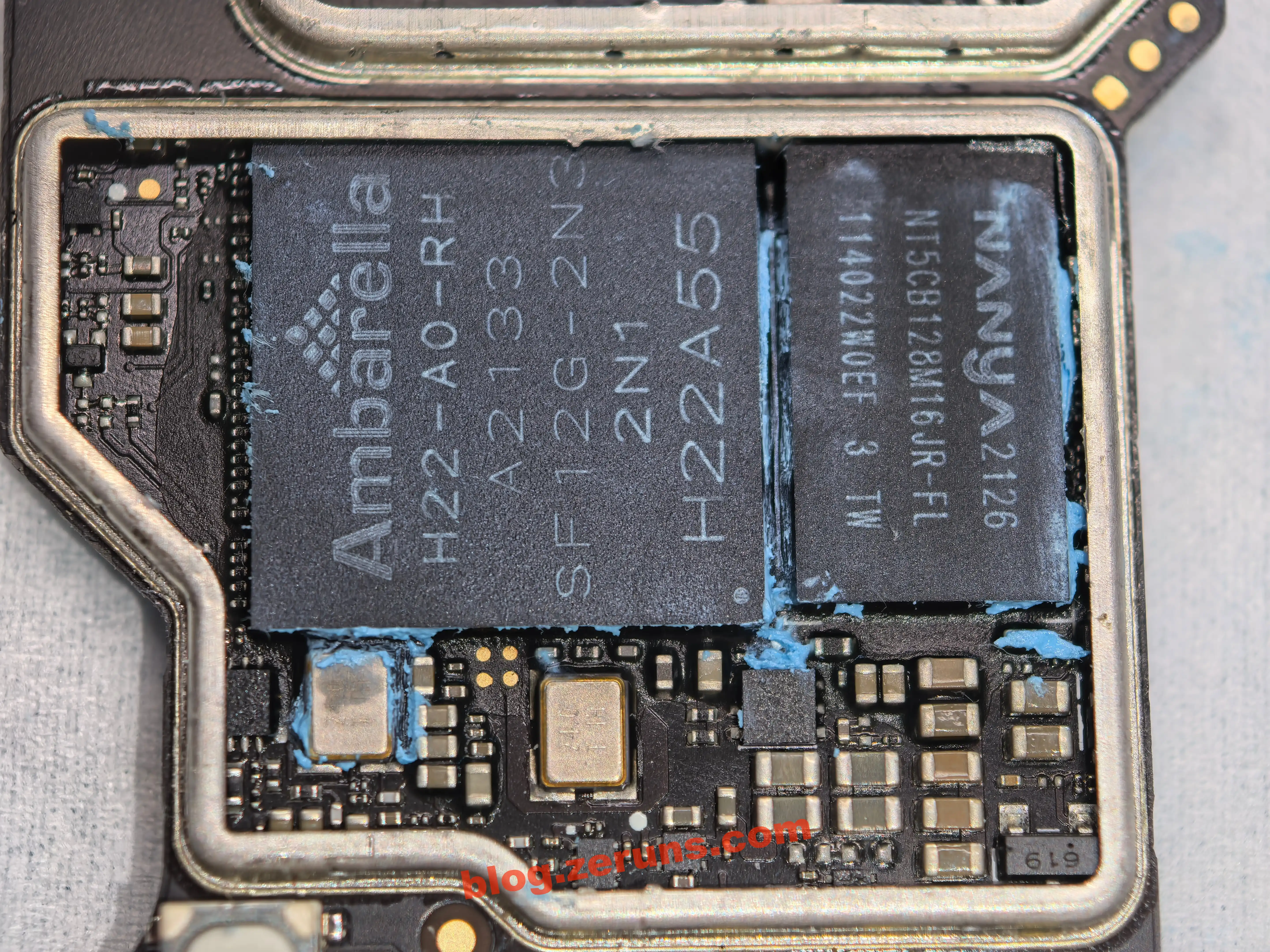
Inside the shield next to the aerial camera connector are two main chips: H22-AO-RH and NT5CB128M16JR-FL.
1. Ambarella H22-A0-RH (Video Processing Chip)
Brand and Positioning: Ambarella is a global leader in video processing chips. The H22 series is its high-performance visual processing solution for consumer drones.
Core Architecture and Process:
- CPU: Quad-core ARM Cortex-A53, up to 1 GHz.
- Process: 14 nm, balancing performance and power efficiency for long-term portable device operation.
- GPU: No discrete GPU specified, but integrates a high-performance video DSP supporting 4K video encoding and decoding.
Video Processing Capabilities:
- Encoding Formats: Supports H.265 (HEVC) and H.264 (AVC), capable of outputting dual video streams (e.g., 4K60fps main stream + mobile-resolution preview stream).
- Resolution and Frame Rate:
- Main Stream: 4K@60fps (HEVC/AVC).
- Auxiliary Stream: Supports real-time mobile-resolution (e.g., 1080p) WiFi live streaming.
- Image Enhancement Technologies:
- 3D Electronic Image Stabilization (EIS): Supports 4K@30fps via dedicated hardware.
- Multi-exposure HDR: Supports 4K@30fps, enhancing dynamic range.
- Distortion and Shutter Correction: Optimizes image quality.
2. Nanya NT5CB128M16JR-FL (DDR Memory Chip)
- Brand and Positioning: Nanya (Nanya Technology) is a well-known memory manufacturer; this model belongs to the DDR3 series.
- Core Specifications:
- Capacity: 128M×16bit (2 Gbit = 256 MB), operating voltage 1.5V.
- Performance: High-speed data throughput to meet the bandwidth demands of the Ambarella H22 for image buffering and algorithm execution.
- Function: Acts as system RAM, providing temporary storage for the video processor to ensure smooth 4K video encoding and real-time image processing.
Together, these two chips form the drone’s visual processing core: Ambarella H22 handles “processing” and intelligent algorithm execution for HD video, while Nanya memory serves as its “temporary warehouse,” enabling DJI’s 4K HD video transmission and intelligent visual features.
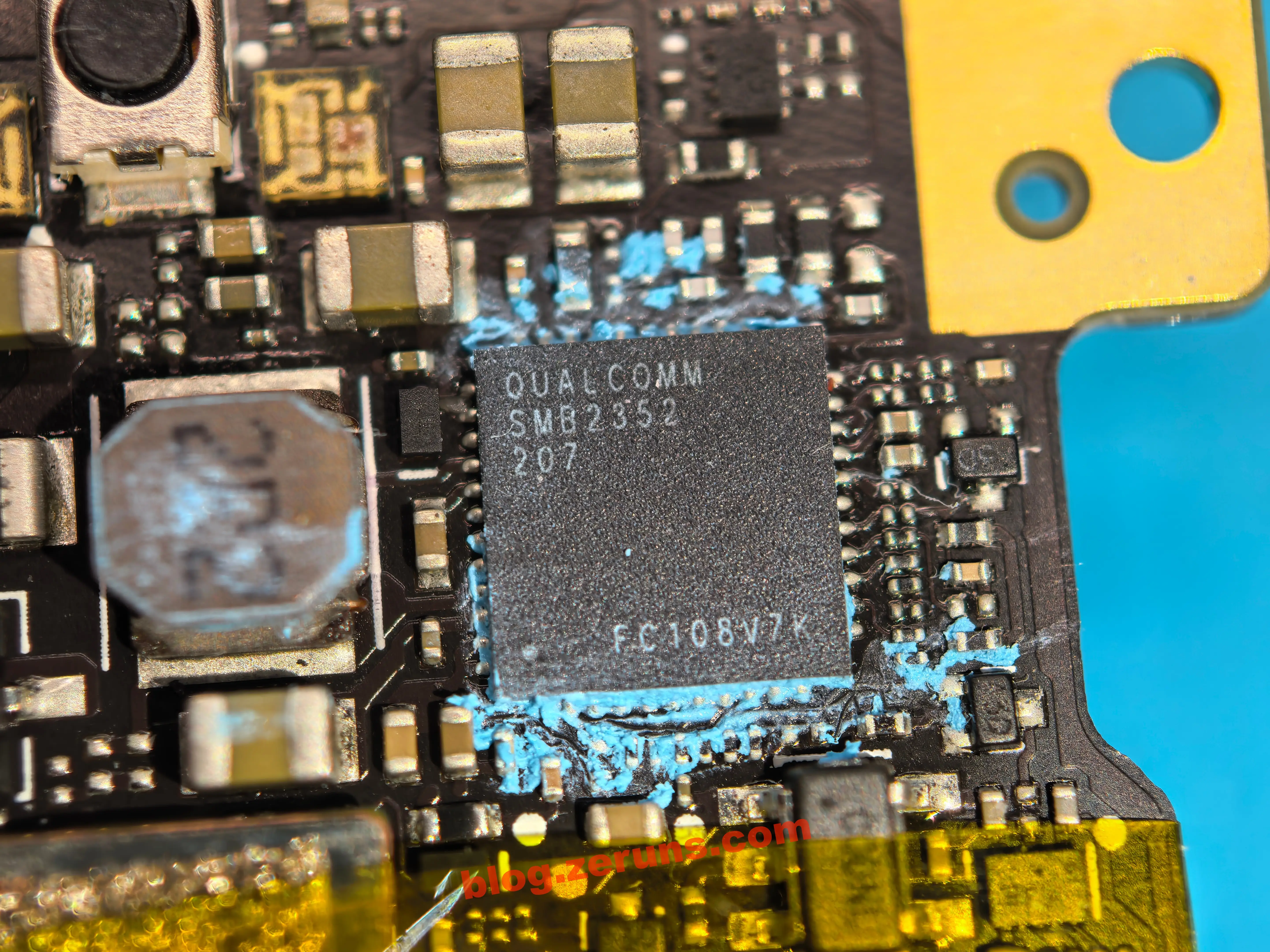
To the right of the Type-C port is a relatively large chip labeled SMB2352.
SMB2352 is a high-efficiency Buck-Boost charging management IC from Qualcomm, designed for two-cell battery applications such as power banks, drones, and portable computers. Key technical specifications:
- Input Voltage Range: 3.3 V to 16.5 V (supports USB Type-C input)
- Output Voltage Range: Buck-Boost regulated, provides 3.3V to 20V system power
- Maximum Charging Current: Up to 6A at battery terminal (programmable)
- Maximum Input Current: 5A (programmable current limit)
- Input Power: Up to 45W
- Efficiency: Typical >90%
- Package: MQFN-57, 5.5 mm × 5.5 mm × 0.6 mm
- Communication & Control: Supports I²C interface for programmable configuration of charging parameters and protection thresholds
- Protection Features: Built-in input overvoltage protection (OVP), input overcurrent protection (OCP), battery overtemperature protection (OTP)
- Protocol Support:
- USB BC 1.2
- Qualcomm Quick Charge 2.0/3.0/4.0
- USB Power Delivery (PD) 3.0 (integrated PD PHY)
- Type-C 1.3 specification
This chip is ideal for high-power-density, high-efficiency portable device charging solutions and allows flexible operation mode adjustment via external controllers.
Recommended Reading
- Recommended High-Value and Affordable VPS/Cloud Servers: https://blog.zeruns.com/archives/383.html
- Minecraft Server Setup Guide: https://blog.zeruns.com/tag/mc/
- [Open Source] 24V3A Flyback Switching Power Supply: https://blog.zeruns.com/archives/910.html
- Mechanical Revolution Code10AI Laptop (Ultra7-255H): Simple Unboxing Review and Disassembly: https://blog.zeruns.com/archives/895.html
- E-commerce Independent Store Setup Guide: WordPress Foreign Trade Website Tutorial: https://blog.zeruns.com/archives/889.html
- Yunyun RCA Cloud App (K8s-based) Tutorial for PHP Website Setup: https://blog.zeruns.com/archives/869.html
English Version of the Article: https://blog.zeruns.top/archives/75.html