开源一款全国产的基于EG1151芯片的大功率可调升降压DCDC电源模块,支持TypeC接口输入,带PD3.1诱骗最高支持48V,还有XT60和DC5.5接口输入,最高输入/输出电压63V,最大输入/输出电流20A,支持过流保护和过温保护,最高效率96.8%。
这款模块使用的元器件全都国产的。
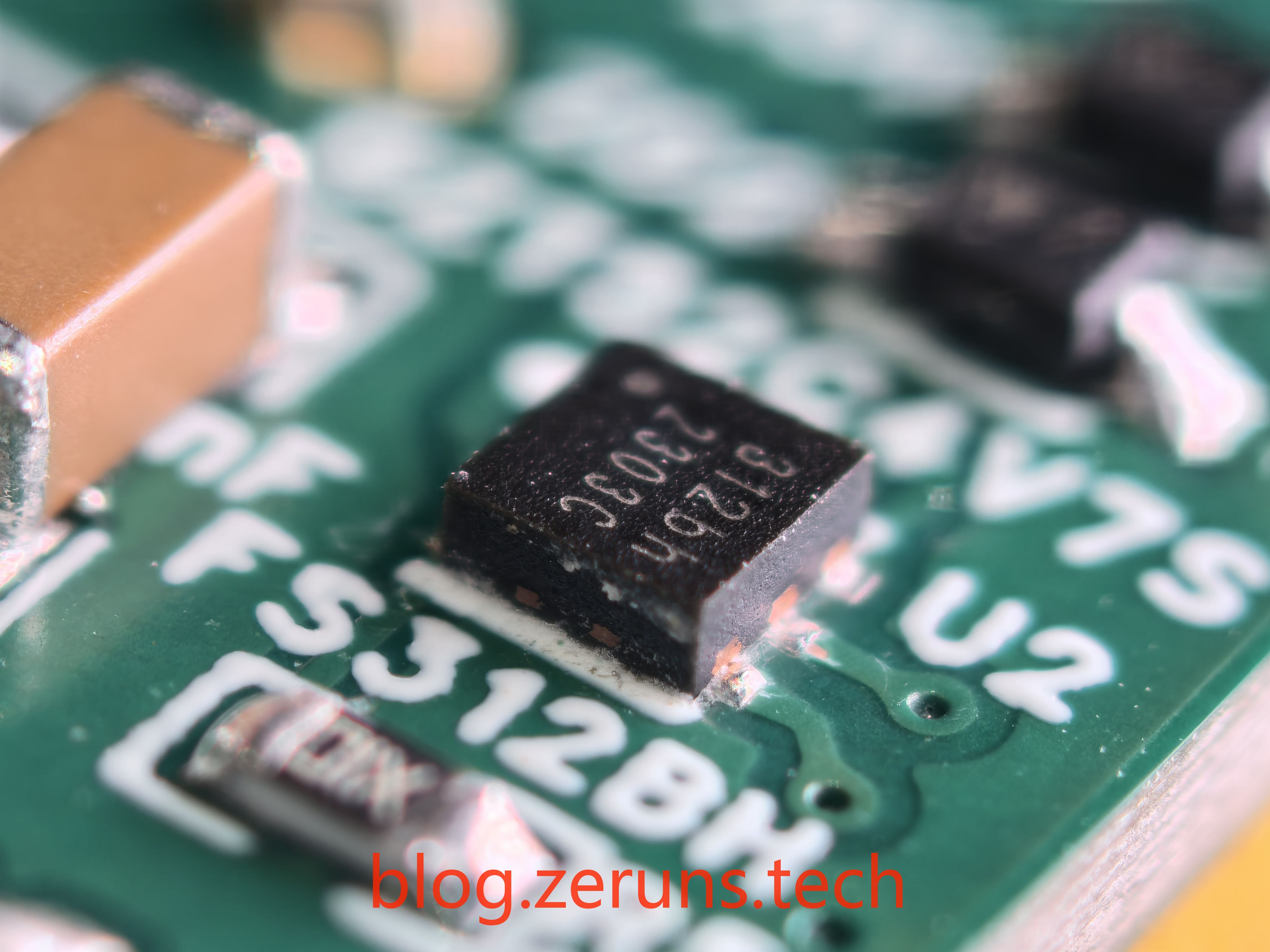
使用的PD3.1诱骗芯片型号为FS312BH,最高可以诱骗PD充电器输出48V,如果充电器不支持这个电压就会自动选取最接近的电压,比如你PD充电器最高支持28V,那就会输出28V。(截止发文时,市场上的PD3.1充电器好像最高才只能输出28V)
如果需要TypeC接口输入28V除了充电器要支持PD3.1 28V,还需要你的数据线有E-mark芯片,并且支持PD3.1 ERP28V协议。
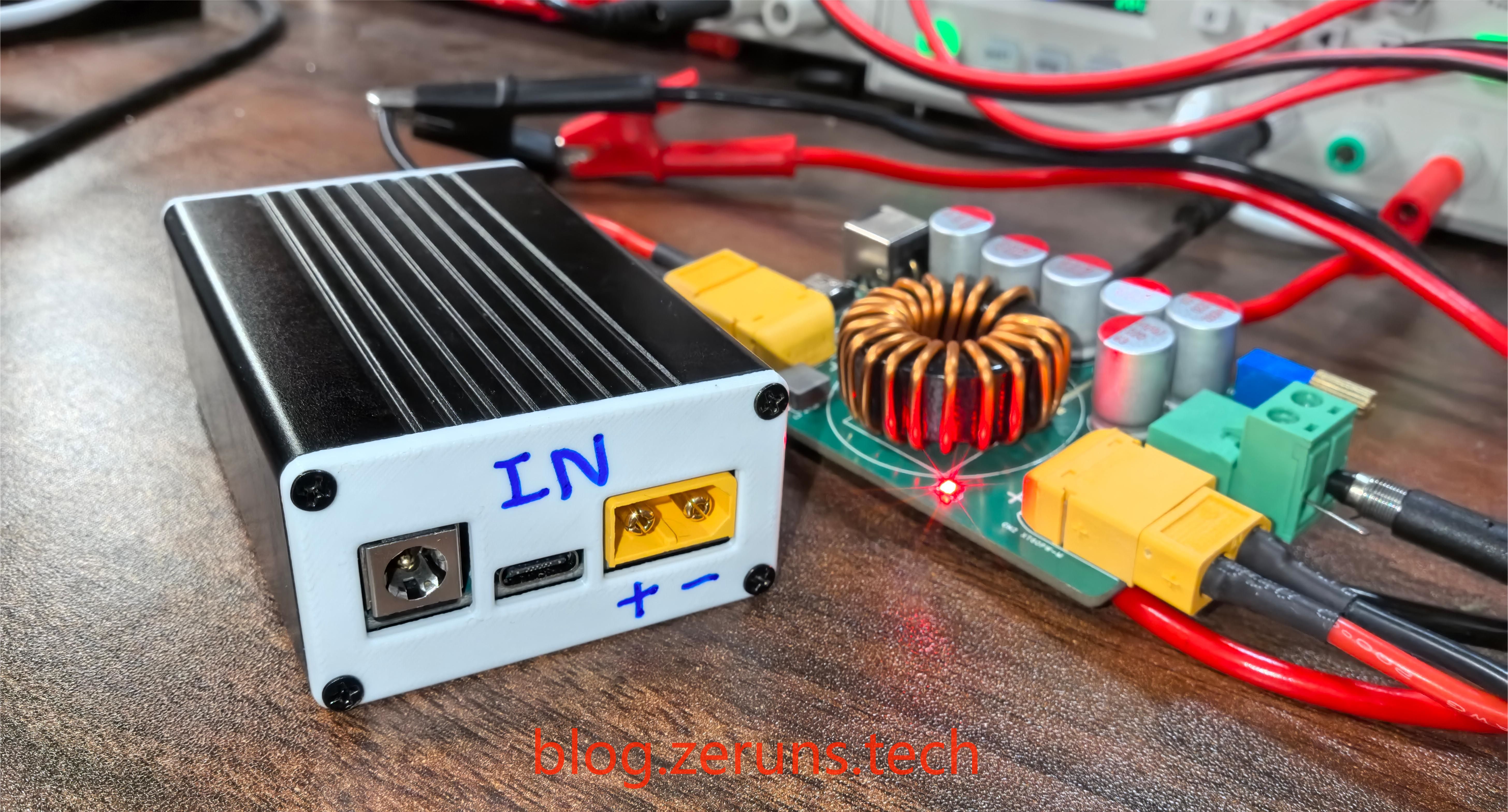
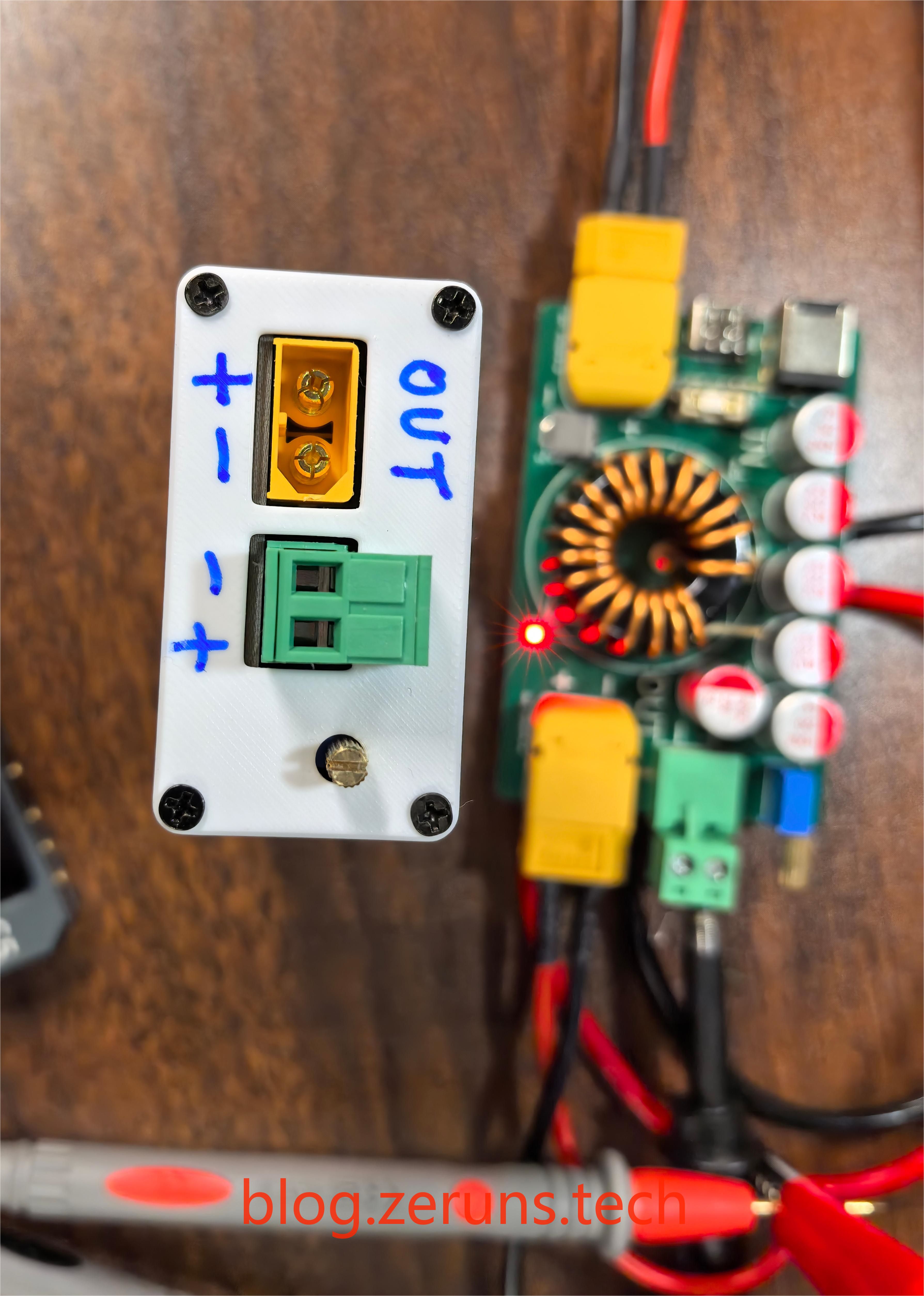
注意:三个输入接口不能同时使用,输入接口间是并联的!
视频演示:https://www.bilibili.com/video/BV1fS411P7Cp/
资料下载链接在文章末尾!
本模块设计最大电流是20A,但实际测试最多只能去到18A左右,18A的时候压降已经比较明显了!
做得一般,大佬们勿喷,如果觉得有哪些地方可以改进一下的可以在评论区提一下建议,欢迎友善交流。
电子/单片机技术交流QQ群:2169025065
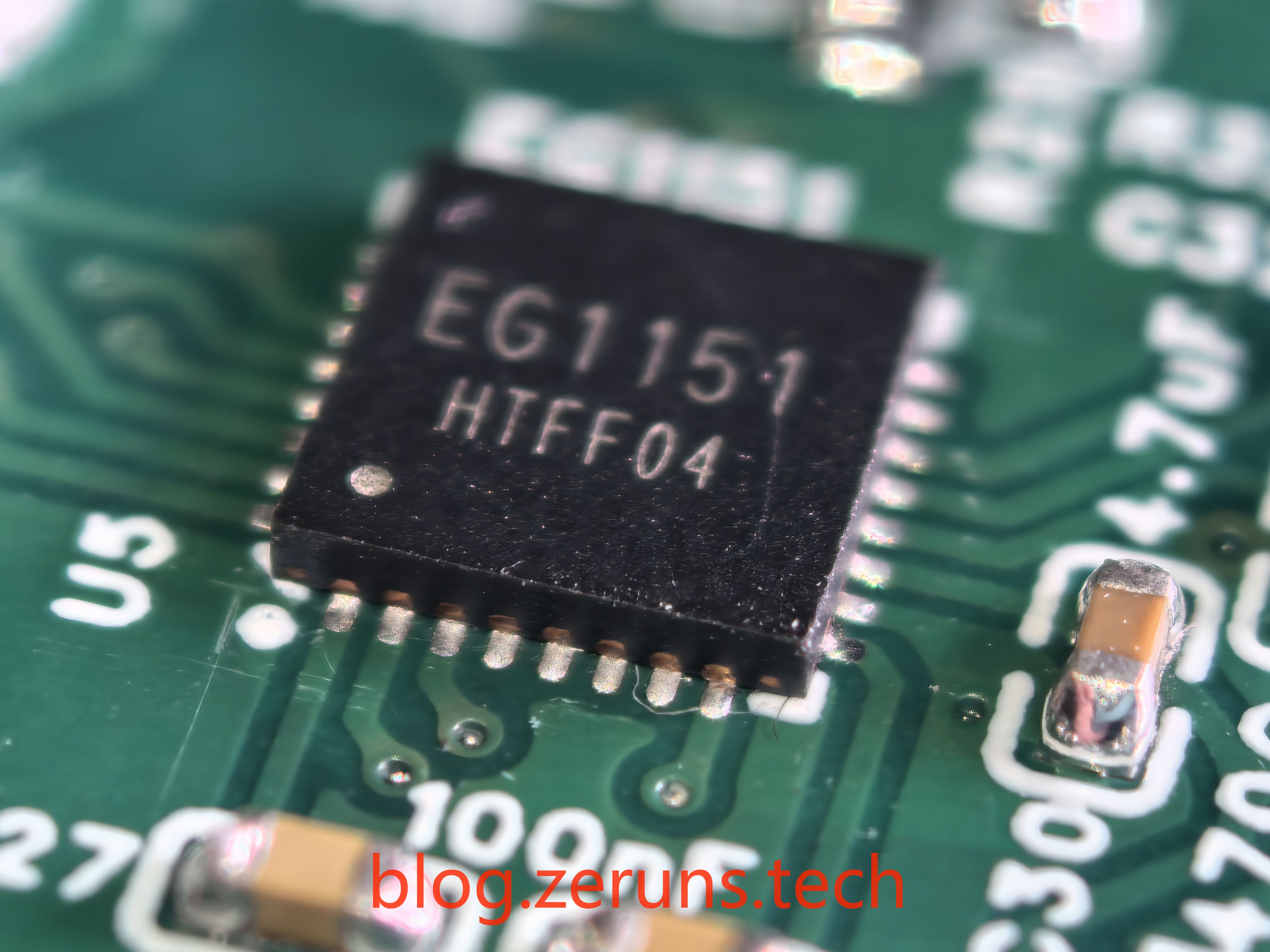
EG1151简介
EG1151 是一款四开关降压-升压型 DC-DC 电源管理芯片。内部集成基准电源、振荡器、误差放大器、限流保护、短路保护、半桥驱动等功能。能根据输入和输出电压的具体关系和不同负载条件采取相应的控制策略。在输入电压的整个波动范围内提供稳定的电压输出。非常适合宽电压范围大电流需要升降压的,特别是电池供电的电压并不恒定的场合,同时支持对蓄电池充电。
特性:
- 宽输入电压范围:7V——150V
- 高效率,可高达 95%
- 欠压保护
- 过温保护
- 支持对蓄电池充电
- 输出短路保护
- 封装形式:QFN32
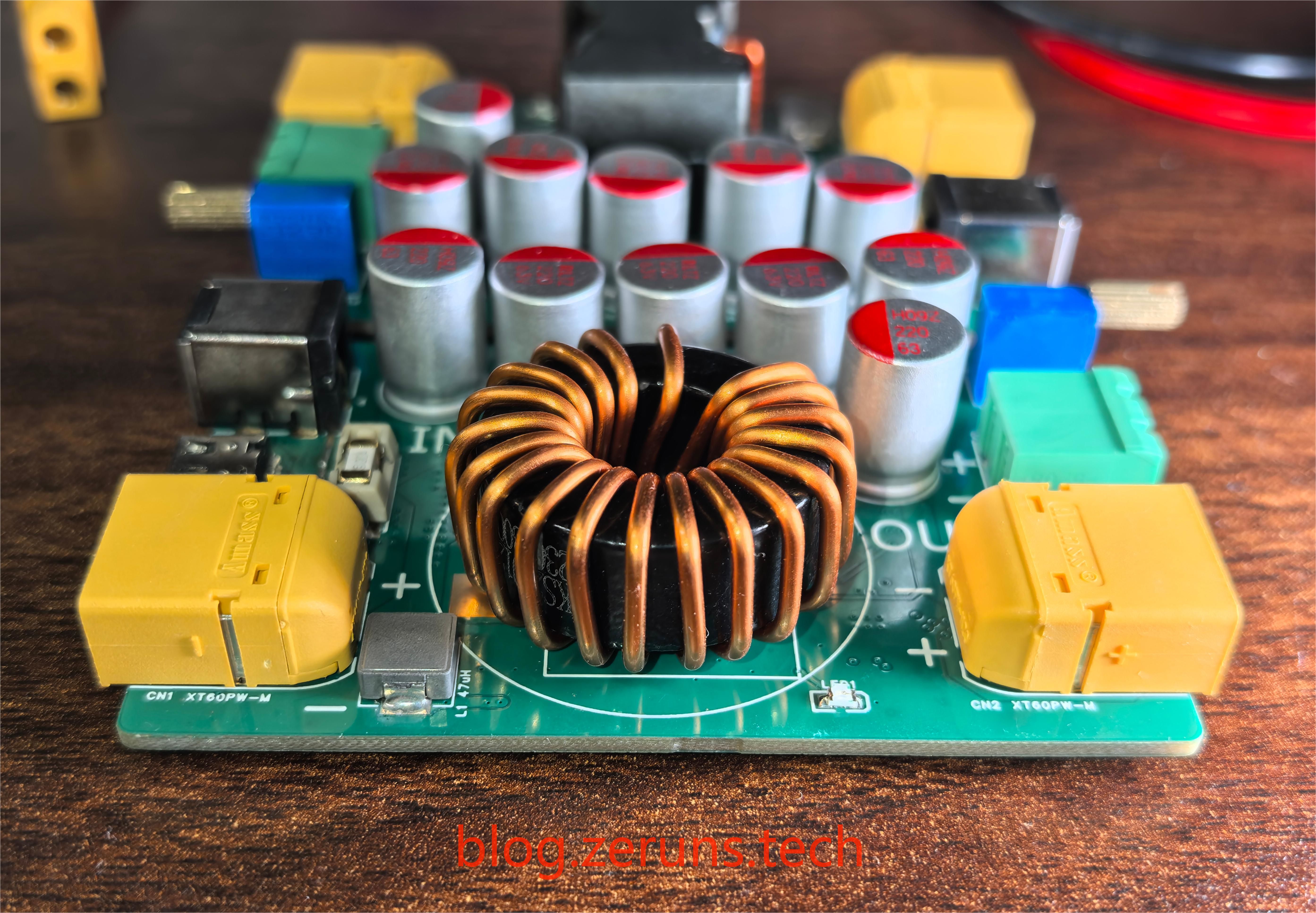
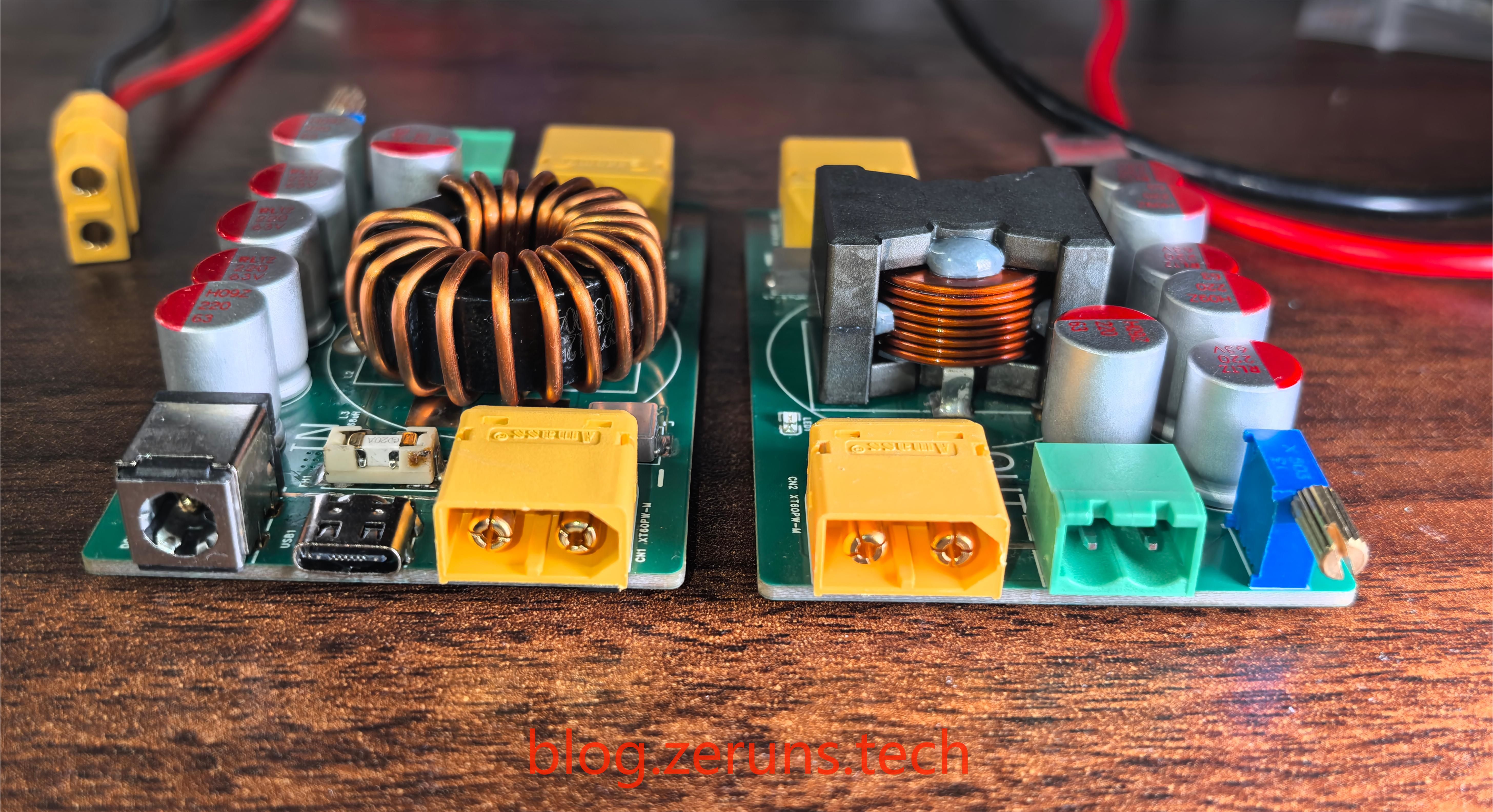
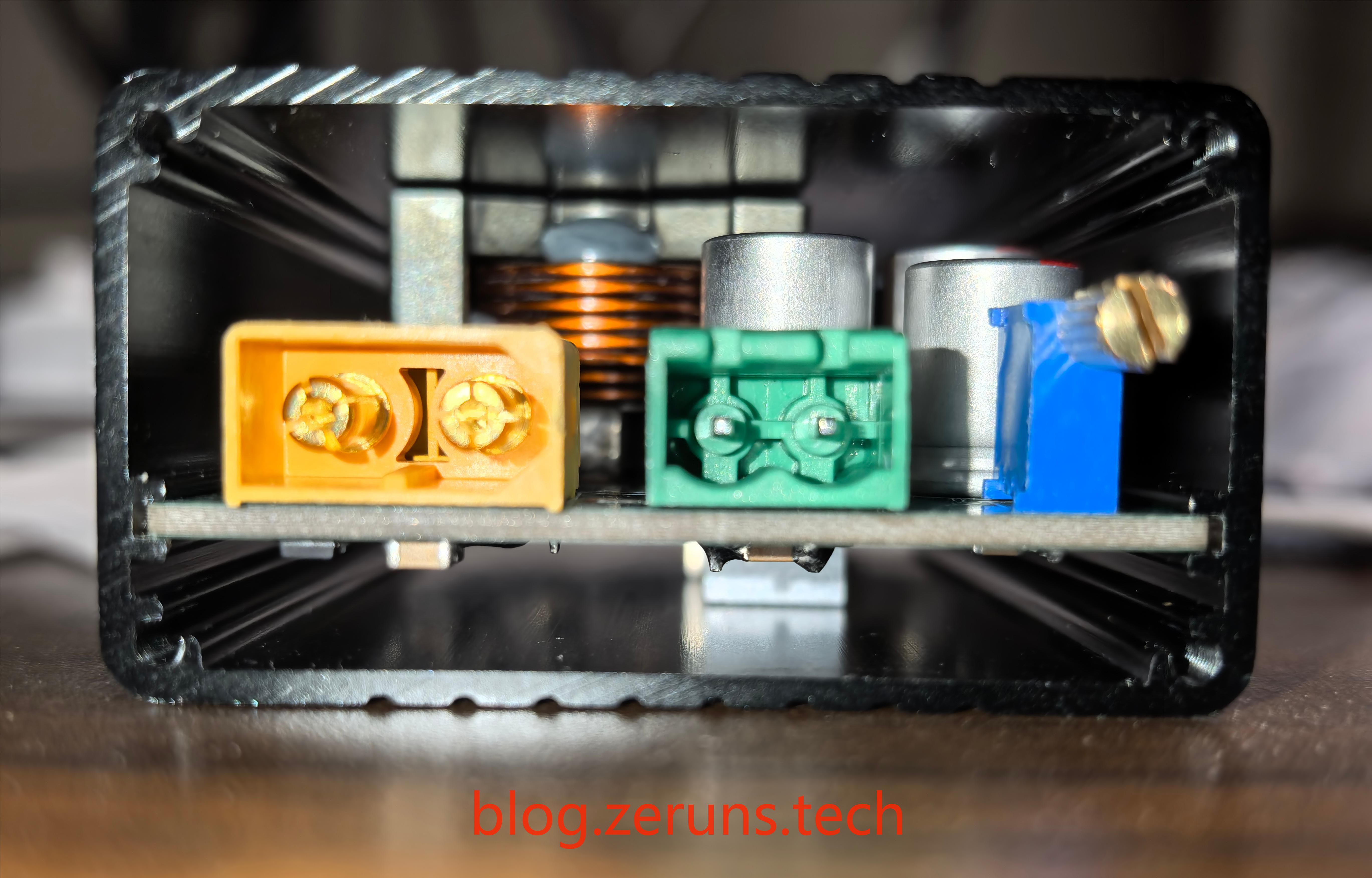
实物图
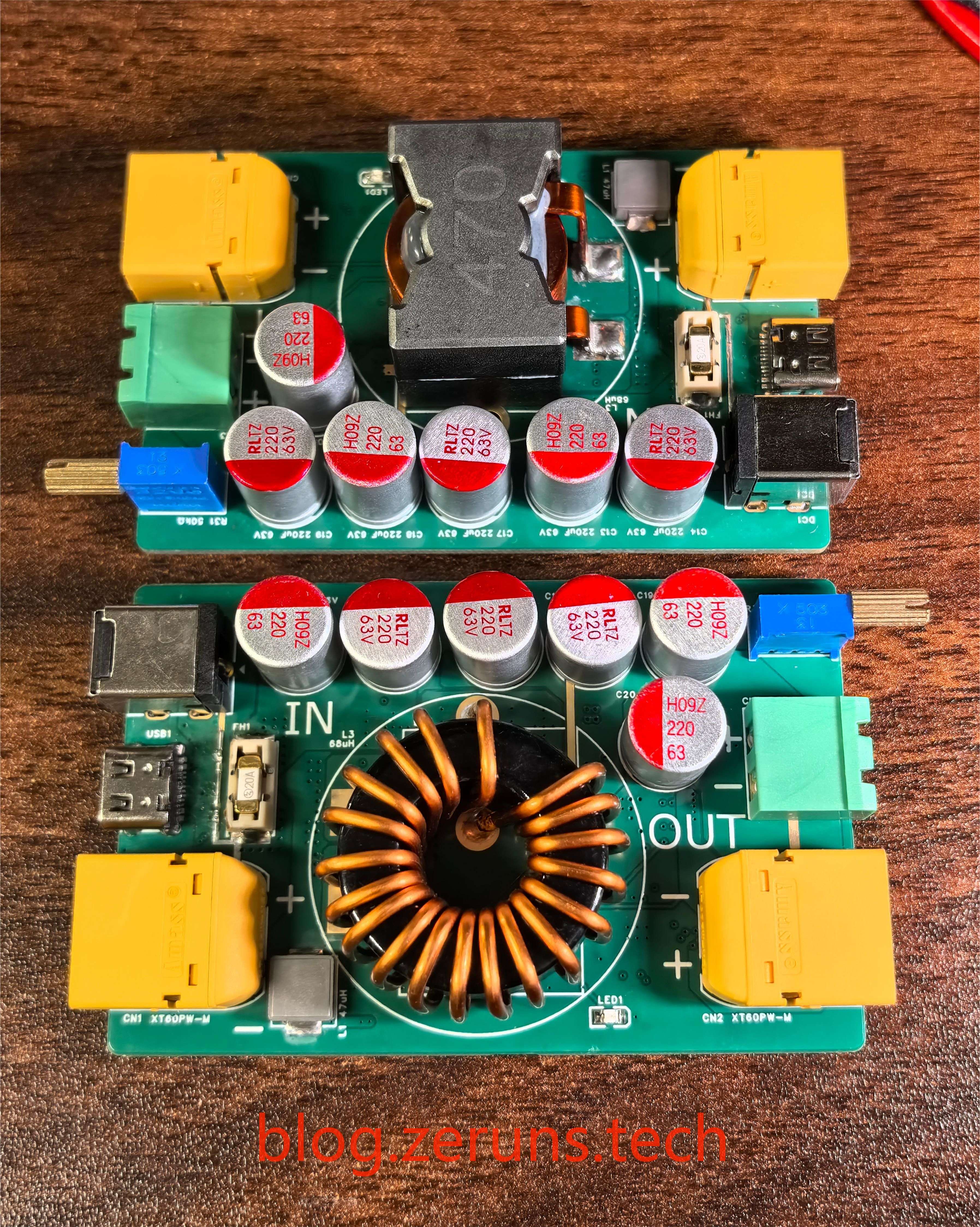
外壳是在淘宝买的铝壳,然后前后盖是自己设计然后3D打印出来的。外壳和前后盖的3D模型也在资料里。
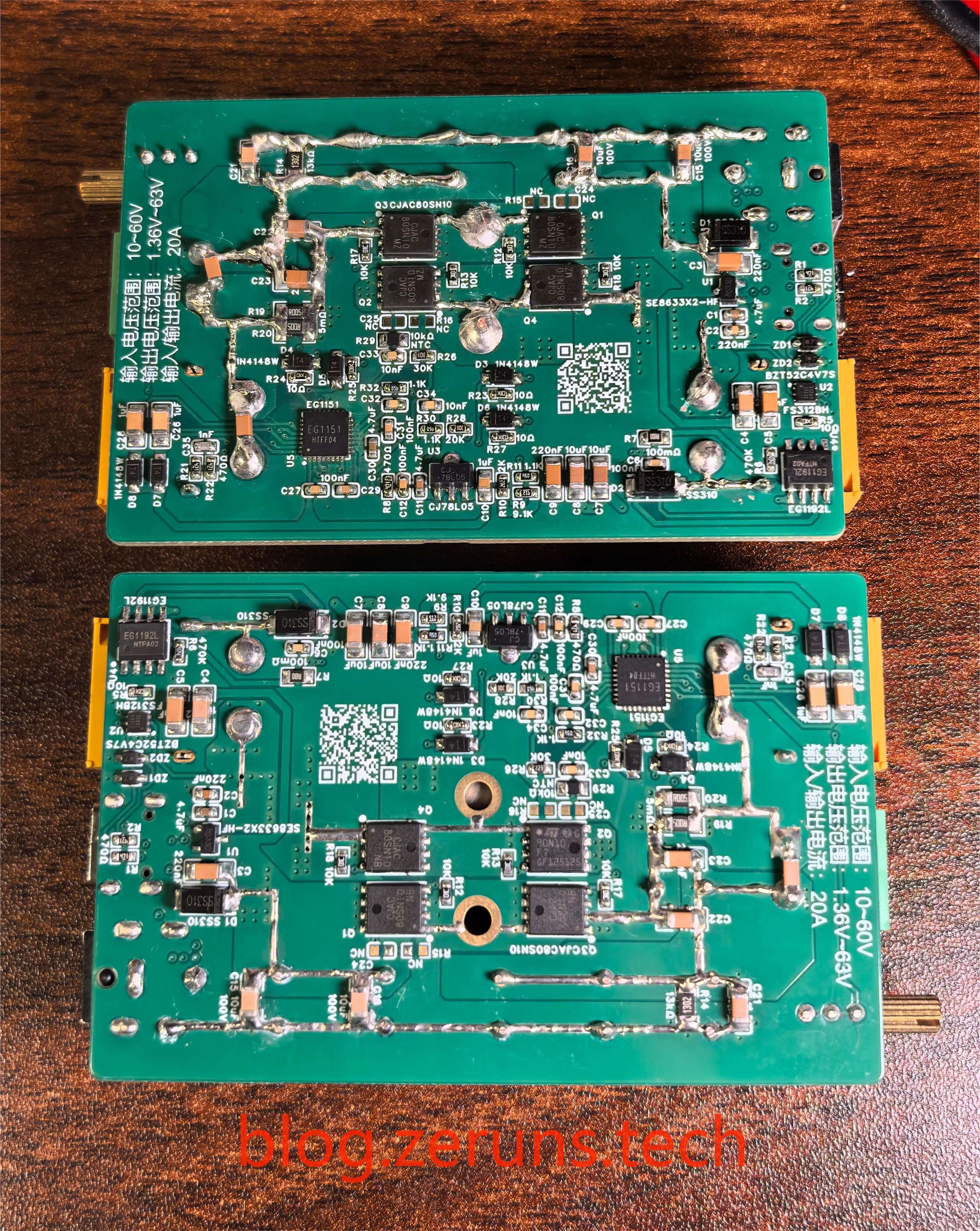
芯片焊接技巧
那个EG1151芯片封装是QFN32,还有FS312BH芯片封装是DFN2X2-6L,这两种封装都很小,比较难焊需要一点技巧。
焊接这两种封装时如果你的PCB是沉金工艺的,要先给焊盘丄锡,如果是镀锡工艺的就给芯片引脚丄锡,注意最好用中低温的焊锡(如果用高温焊锡很难焊),中间的焊盘不要上太多锡,上一点点就行,不然会把芯片顶起来导致四周引脚接触不了,如果上多了就把烙铁清理干净慢慢把锡吸走,或者用吸锡带,上好锡后给焊盘挤一点焊油,把芯片放上去,然后放到加热台上,或者用热风枪吹,锡融化后用镊子轻轻动一下芯片,如果会自动归位那就可以了,等凉了后接着检查一下有没有连锡,连锡了就用烙铁处理一下。
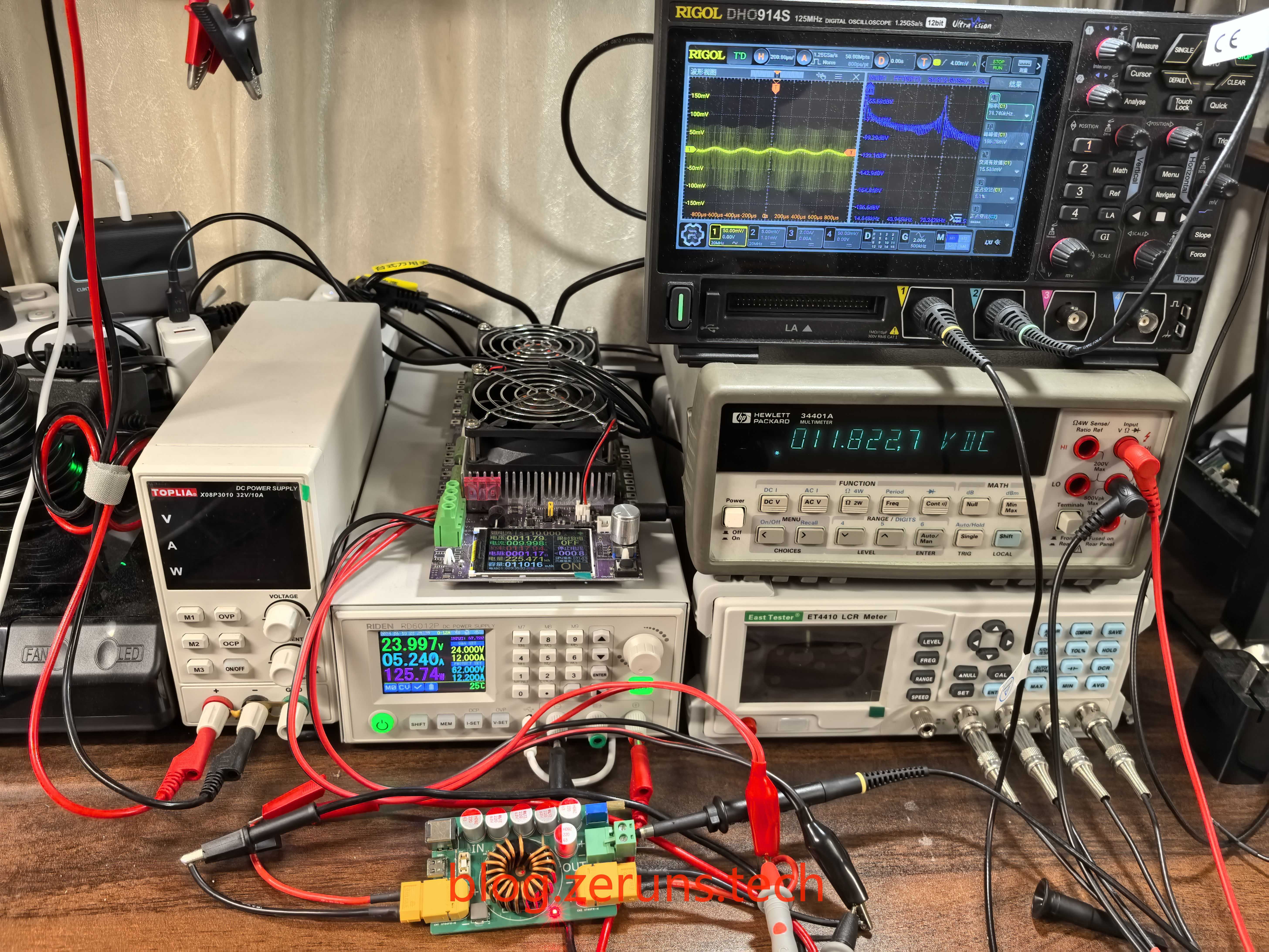
测试
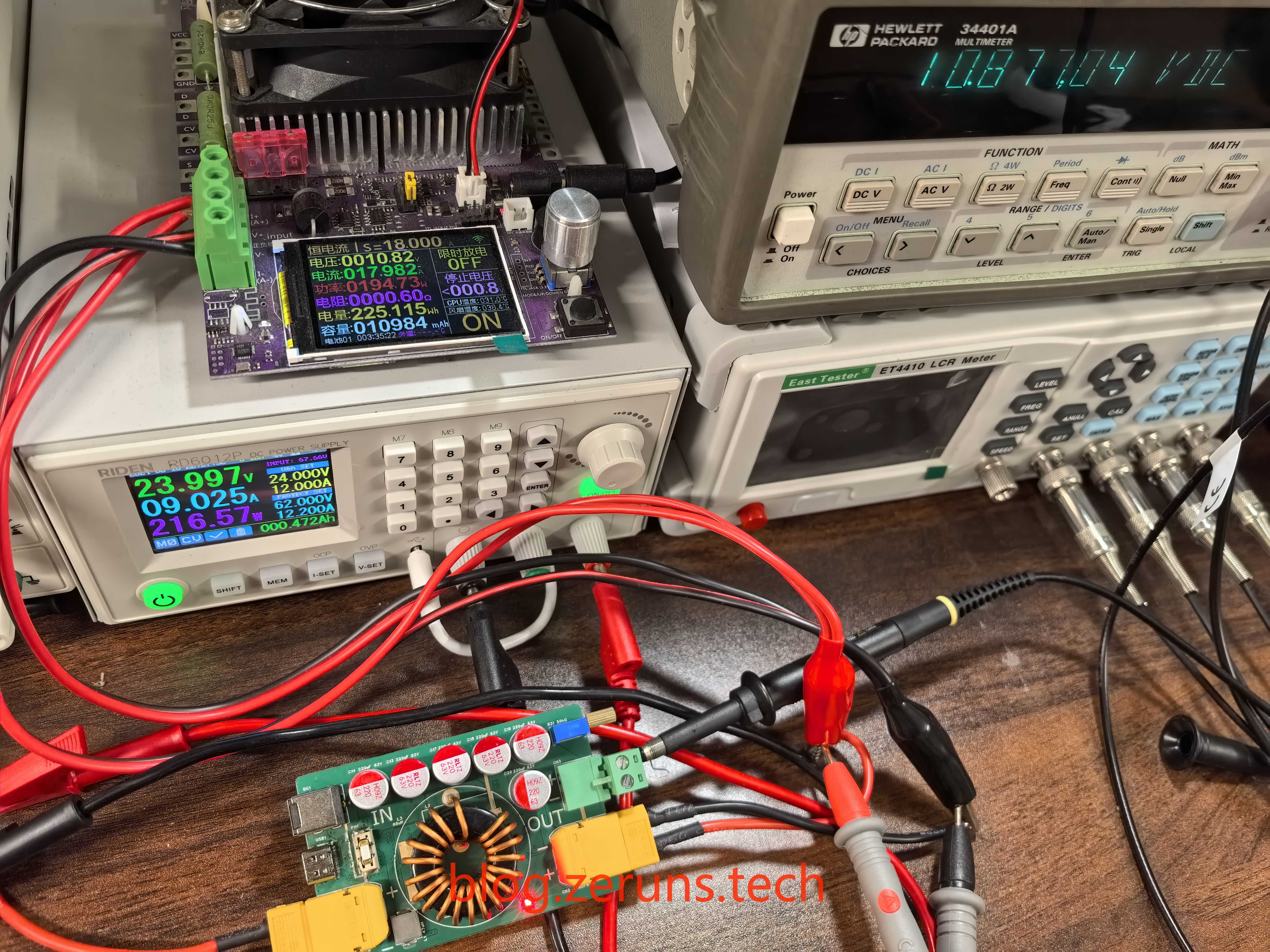
使用XT60接口输入24V电,XT60输出接口接万用表和电子负载。
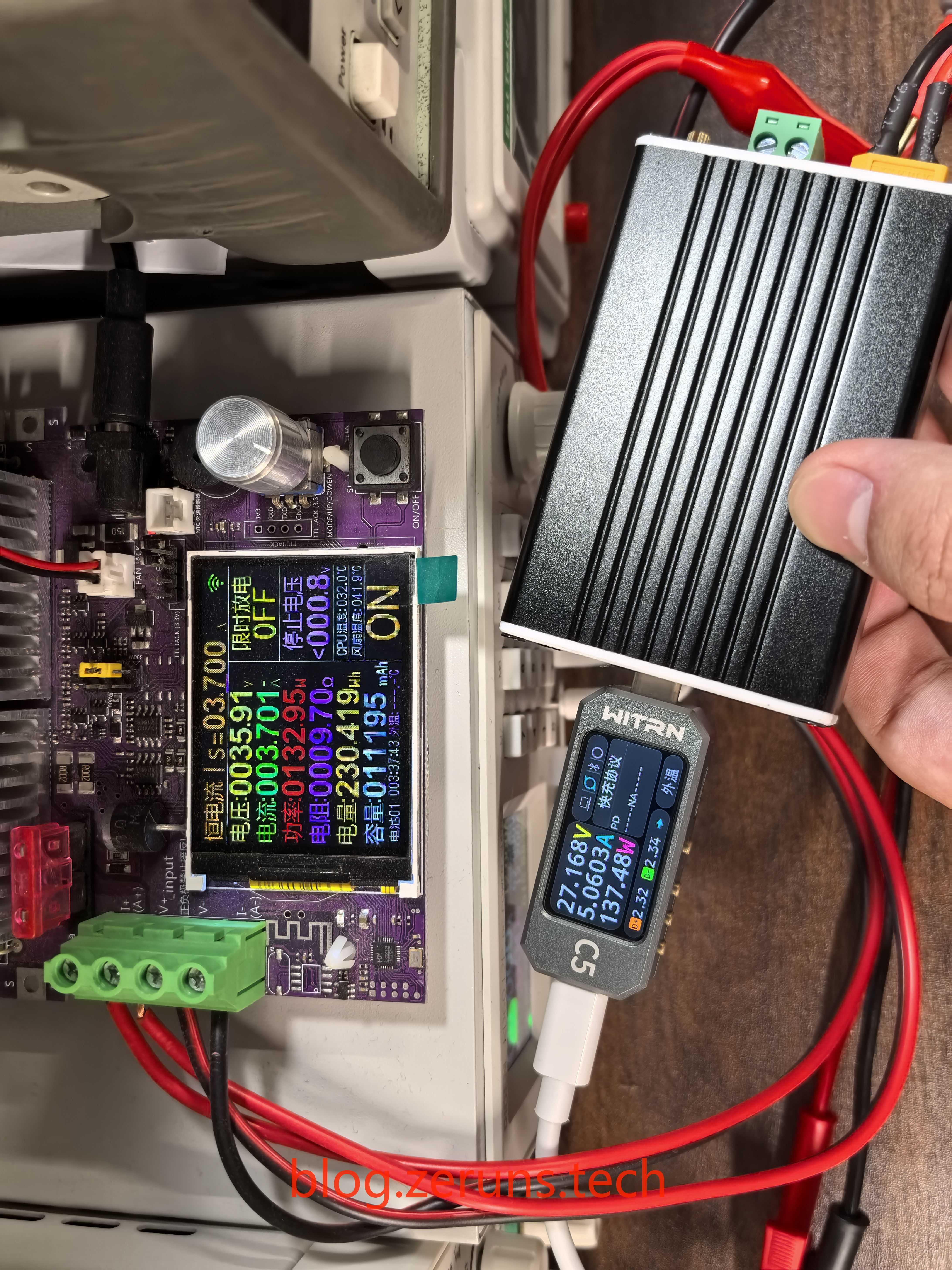
使用TypeC接口输入,接酷态科的140W PD3.1充电器,可以看到成功诱骗28V电压。
最高可以输出63V。
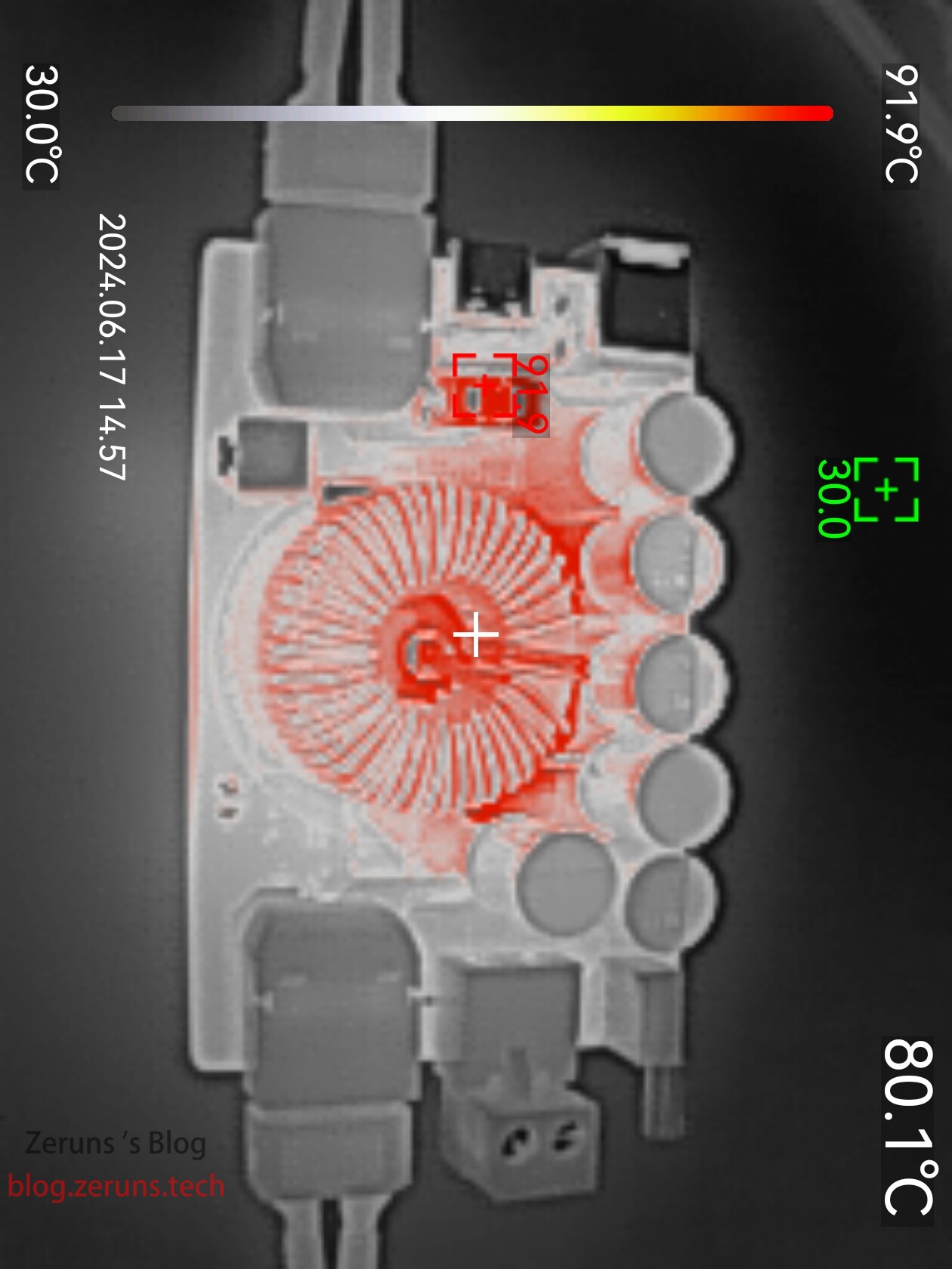
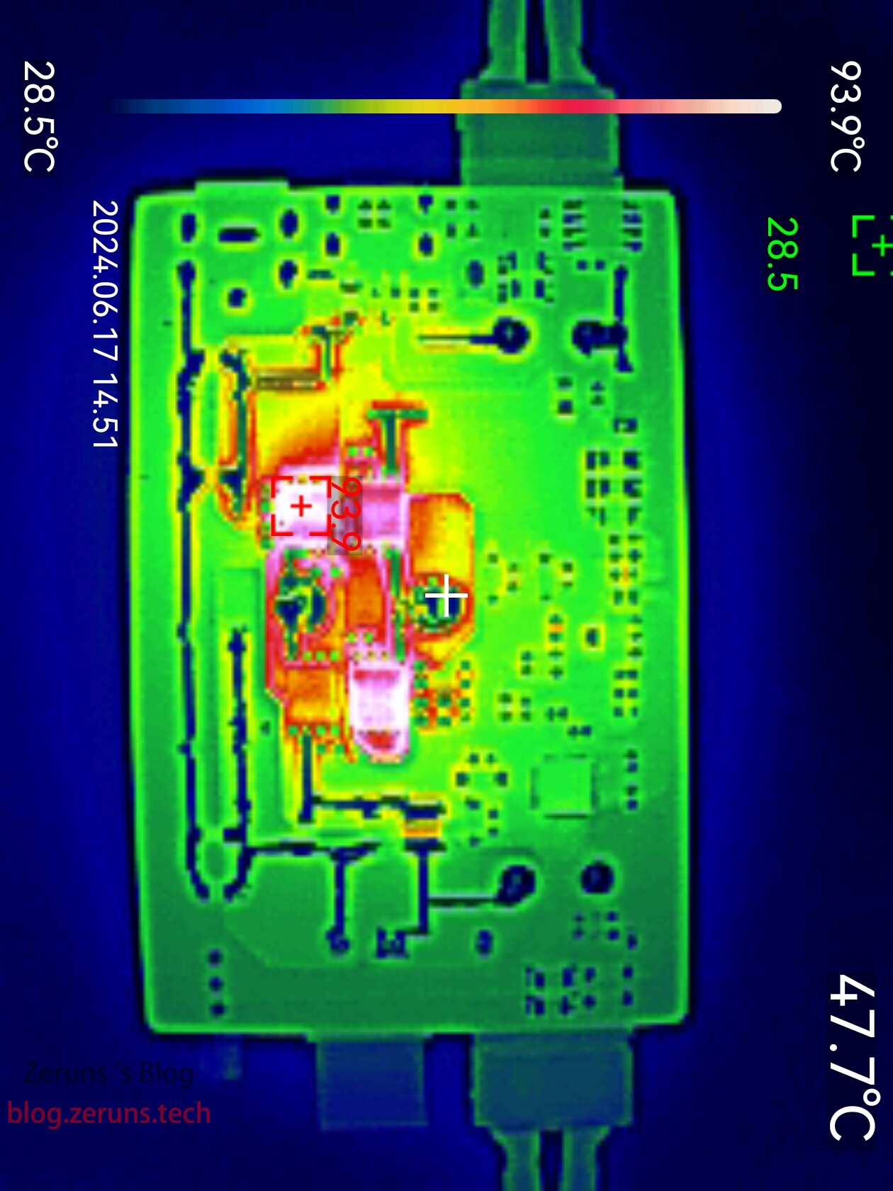
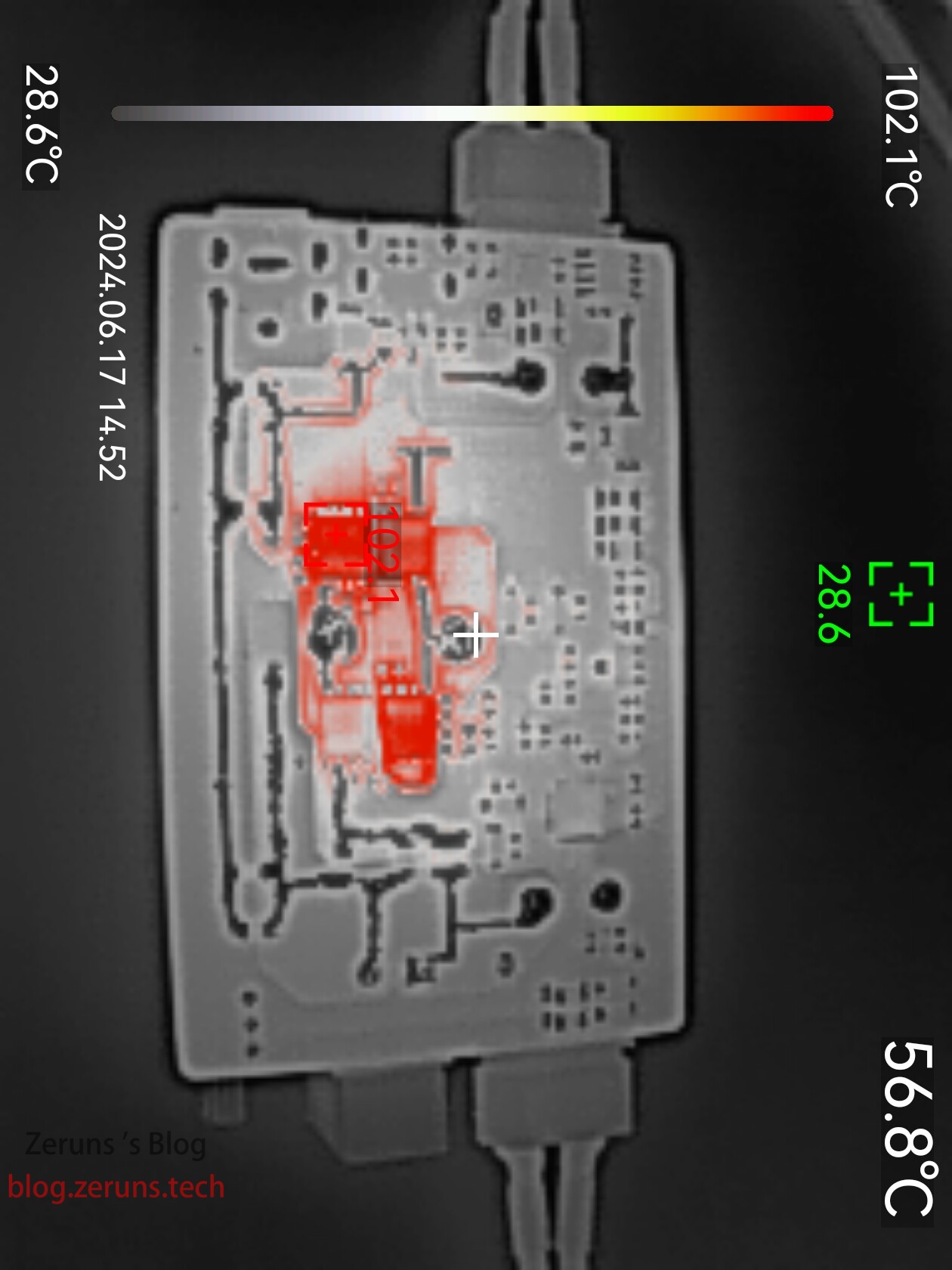
输出10A电流10分钟后的模块热成像图像,MOS管温度在100度左右,保险丝和保险座的接触电阻可能大了一点,所以保险丝那发热也有点大:
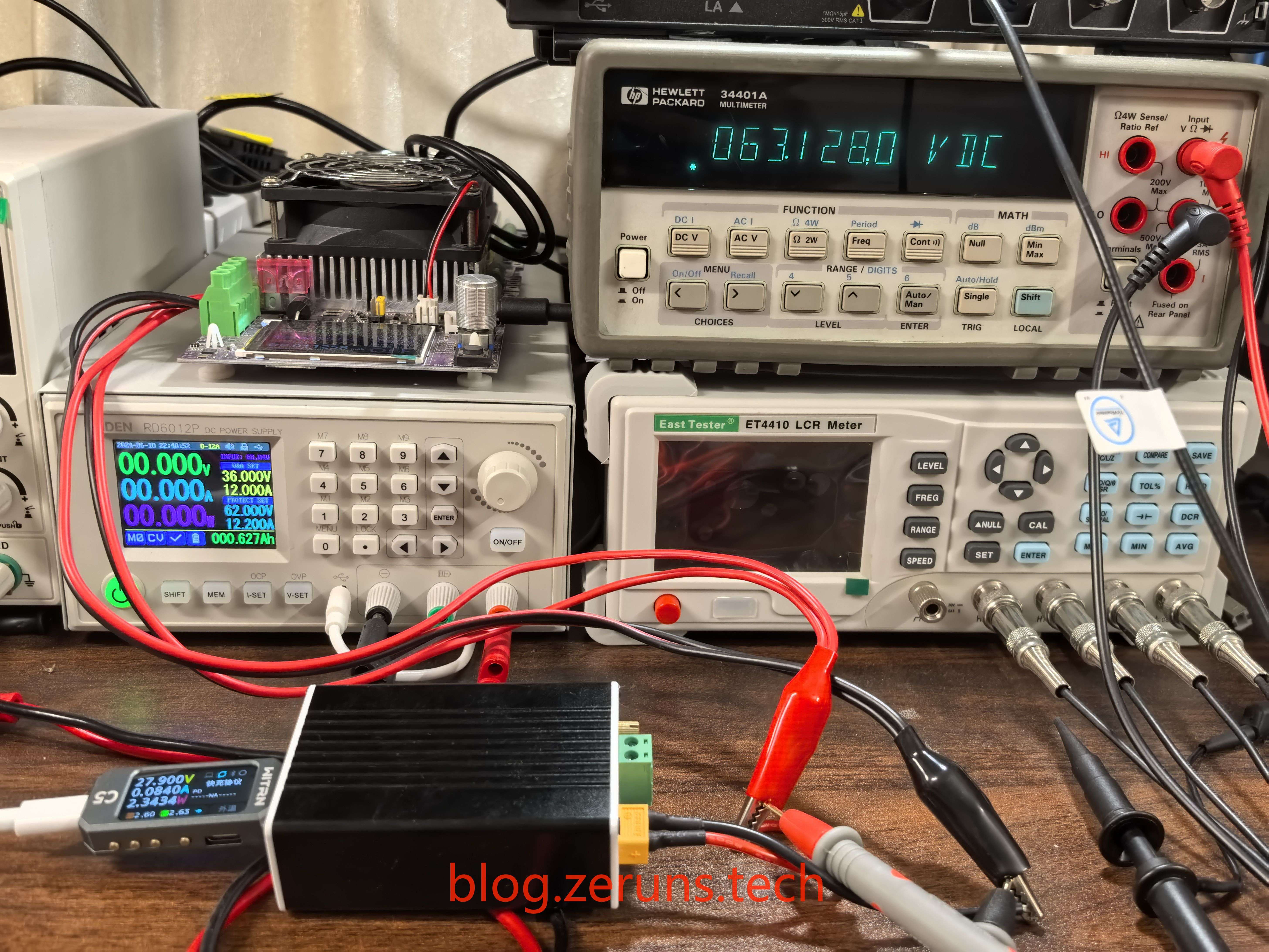
用到的测试设备:
- 惠普34401A六位半万用表:https://blog.zeruns.com/archives/772.html
- 睿登RD6012P数控可调电源:https://blog.zeruns.com/archives/740.html
- 普源(RIGOL) DHO914S示波器:https://blog.zeruns.com/archives/764.html
- 炬为电子负载:https://s.click.taobao.com/EdLEpkt
- 优利德UTi261M热成像仪开箱测评:https://blog.zeruns.com/archives/798.html
转换效率测试
测试得到的最高效率为96.869%。
测试数据如下表:
| 输入电压(V) | 输入电流(A) | 输入功率(W) | 输出电压(V) | 输出电流(A) | 输出功率(W) | 转换效率(%) |
|---|---|---|---|---|---|---|
| 36.000 | 6.932 | 249.552 | 48.194 | 4.996 | 240.777 | 96.484 |
| 60.000 | 6.264 | 375.840 | 35.669 | 9.995 | 356.512 | 94.857 |
| 48.000 | 9.434 | 452.832 | 28.841 | 14.993 | 432.413 | 95.491 |
| 60.000 | 5.941 | 356.460 | 18.430 | 17.988 | 331.519 | 93.003 |
| 60.000 | 4.270 | 256.200 | 12.129 | 18.990 | 230.330 | 89.902 |
| 12.001 | 10.913 | 130.967 | 24.003 | 5.002 | 120.063 | 91.674 |
| 25.000 | 9.915 | 247.875 | 23.749 | 10.008 | 237.680 | 95.887 |
| 12.004 | 9.889 | 118.708 | 36.068 | 3.002 | 108.276 | 91.213 |
| 12.004 | 2.291 | 27.501 | 5.070 | 5.000 | 25.350 | 92.178 |
| 12.004 | 9.130 | 109.597 | 10.116 | 10.013 | 101.292 | 92.422 |
| 48.000 | 7.812 | 374.976 | 36.188 | 10.005 | 362.061 | 96.556 |
| 48.000 | 8.658 | 415.584 | 50.315 | 8.001 | 402.570 | 96.869 |
纹波测试
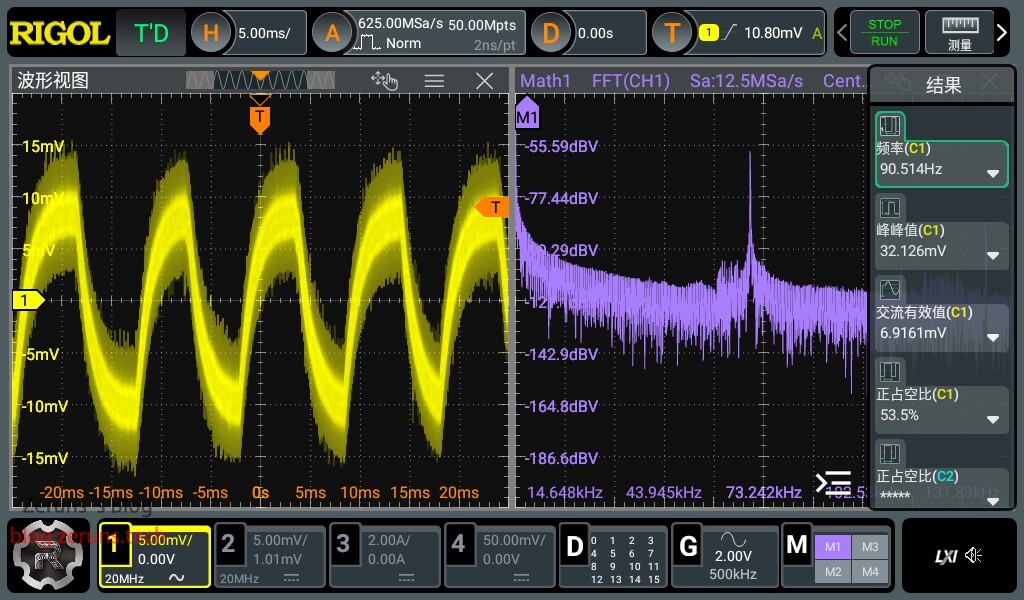
输出12V空载时的纹波峰峰值在32mV左右:
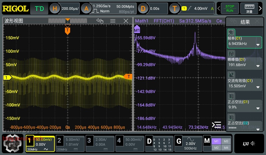
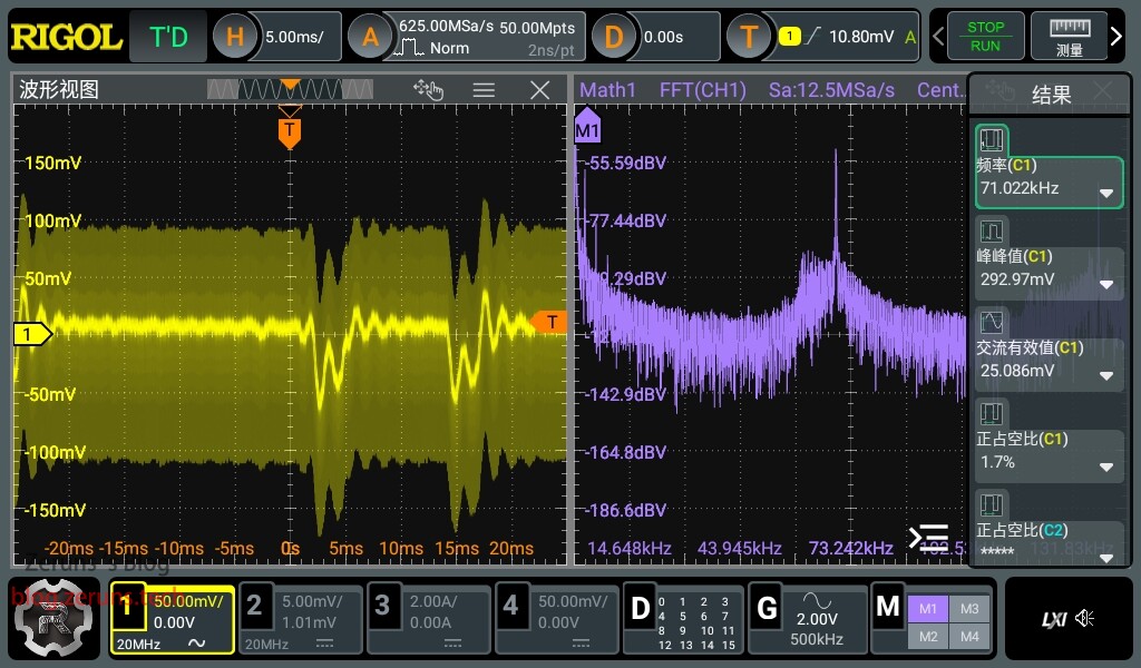
输出12V10A空载时的纹波峰峰值在191mV左右:
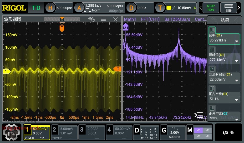
输出12V15A时的纹波峰峰值在277mV左右:
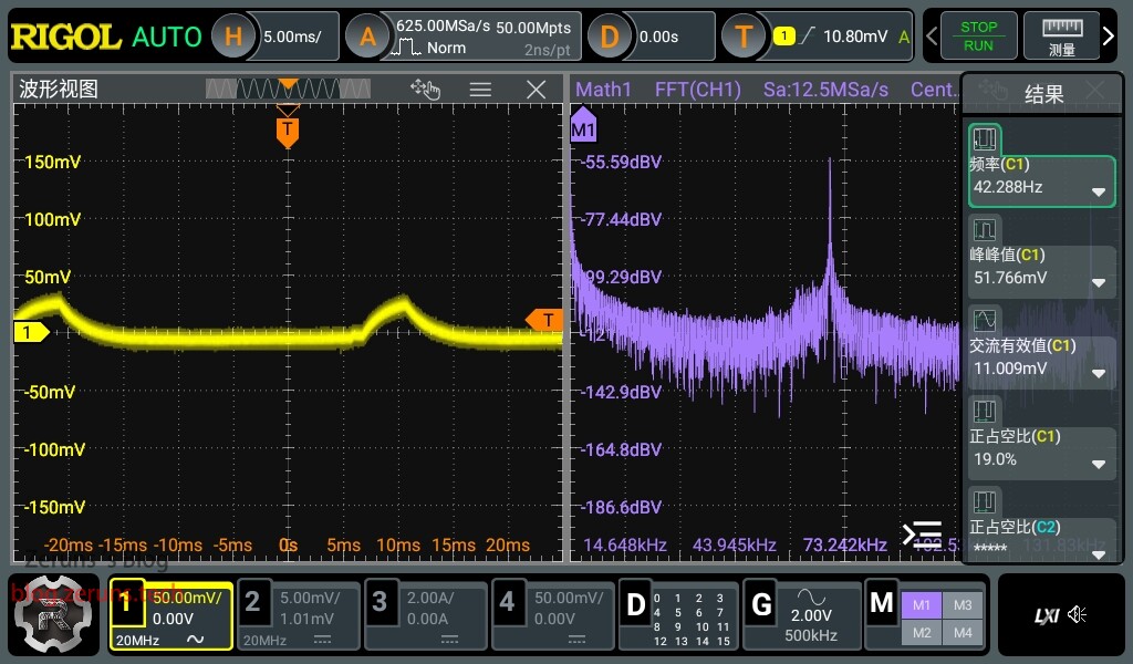
输出36V空载时的纹波峰峰值在51mV左右:
输出36V3A时的纹波峰峰值在292mV左右:
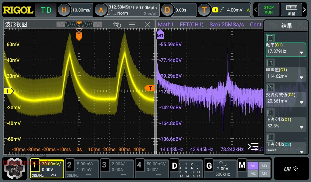
输出60V空载时的纹波峰峰值在114mV左右:
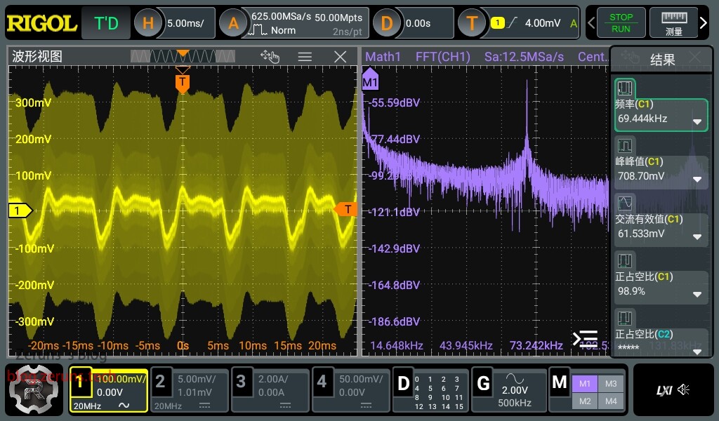
输出60V3A时的纹波峰峰值在708mV左右:
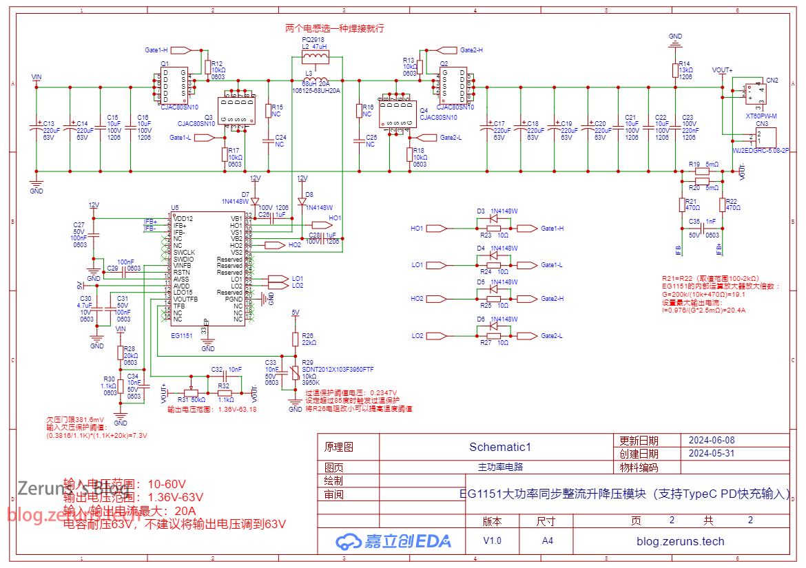
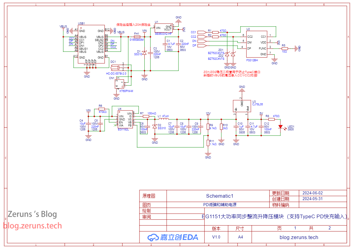
原理图
主功率电路:
PD诱骗和辅助电源电路:
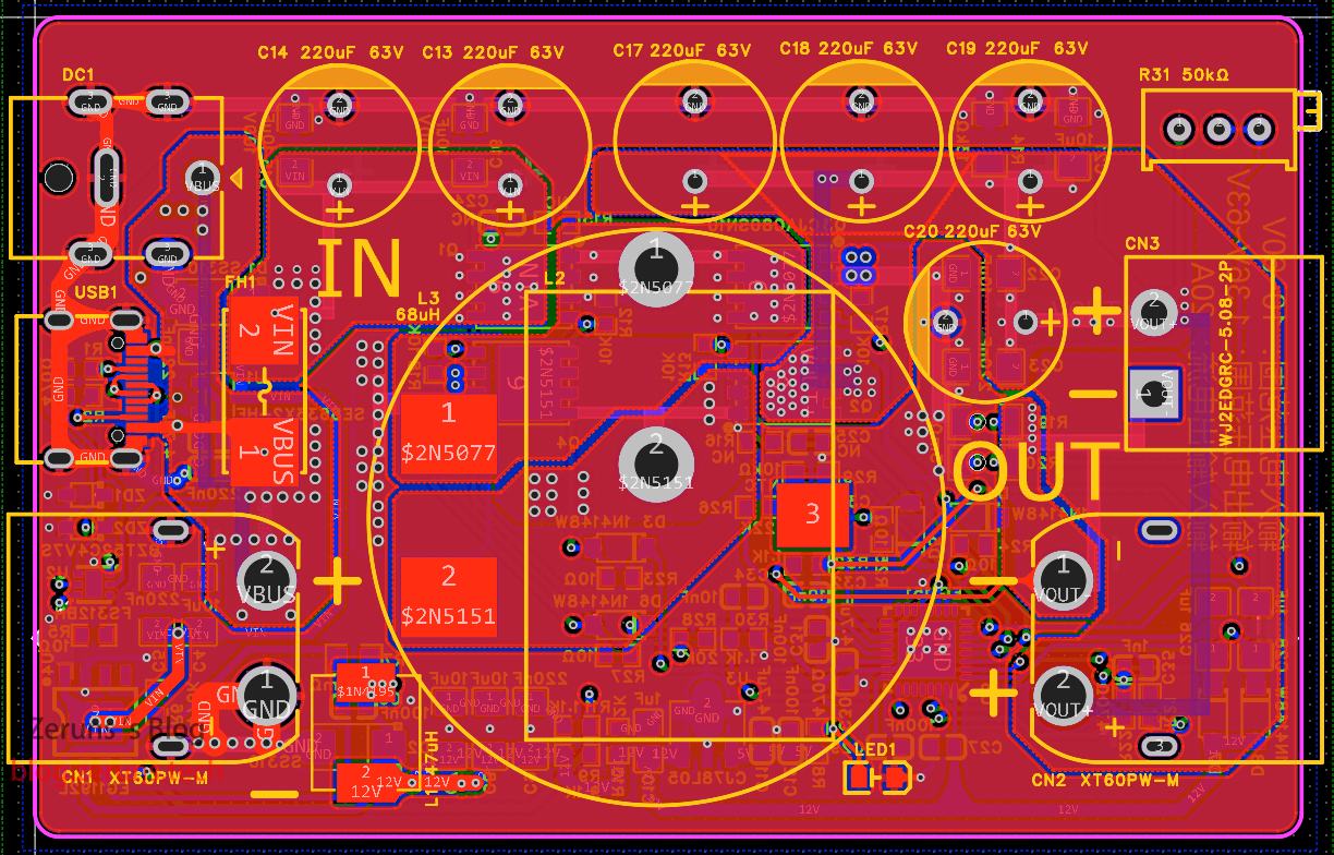
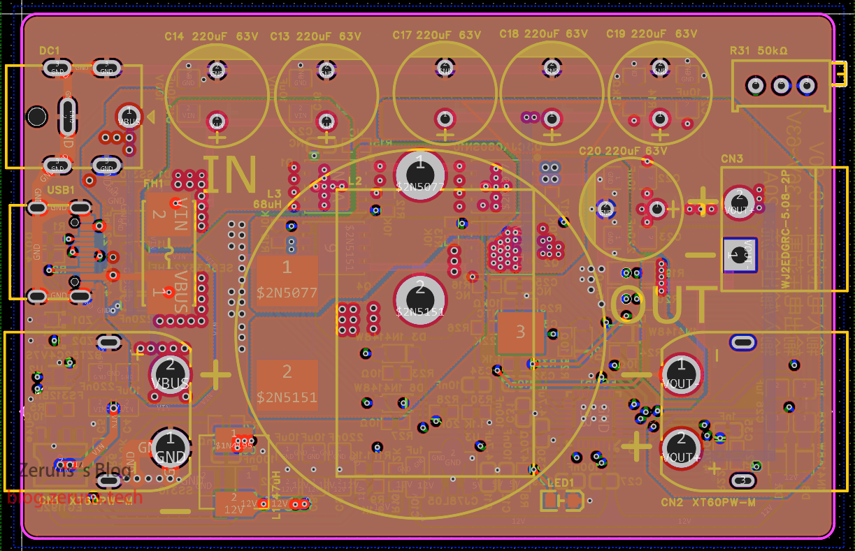
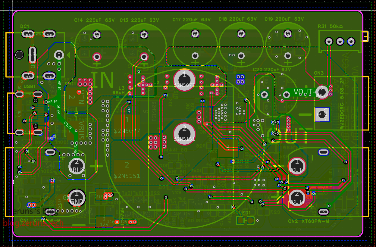
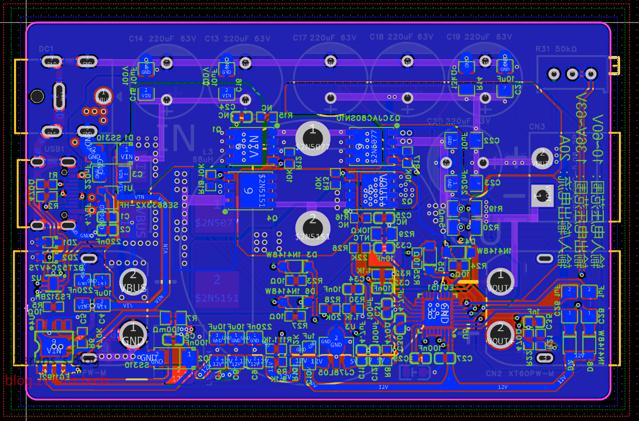
PCB
顶层:
内层1:
内层2:
底层:
元件购买地址
这个项目用到的大部分元件购买地址都在这里:
- 0603电阻电容样品本:https://s.click.taobao.com/SXT7pkt
- TypeC母座 16P:https://s.click.taobao.com/vjLRskt
- EG1151芯片:https://s.click.taobao.com/le3gAkt
- EG1192L芯片:https://s.click.taobao.com/pG2gAkt
- CJAC80SN10 MOS管:https://s.click.taobao.com/aPsWWlt
- XT60PW接口:https://s.click.taobao.com/6jZ7pkt
- 扁平线电感PQ2918 47μH:https://s.click.taobao.com/RDuLHkt
- 磁环电感 卧式 68μH 20A:https://s.click.taobao.com/8JHHcjt
- 铝合金外壳:https://s.click.taobao.com/fYK0zbt
建议在立创商城里购买元器件:https://activity.szlcsc.com/invite/D03E5B9CEAAE70A4.html
在立创开源链接里的BOM表那点立即到立创商城下单可将用到的元器件一键导入到购物车。
资料下载地址
下面下载链接包含:立创EDA工程、原理图PDF文件、用到的各种芯片的数据手册、外壳3D模型文件。
百度网盘下载链接:https://pan.baidu.com/s/1gNl48K25p6Pr3gi9lsyMAg?pwd=tmsv 提取码:tmsv
123云盘下载链接:https://www.123pan.com/s/2Y9Djv-r3tvH.html 提取码:0cGK
如果觉得对你有用的可以进去上面的123云盘链接里给我打赏,如果是微信文章(公众号:zeruns-gzh)的也可以点击文章下方的喜欢作者给我打赏,谢谢。
其他开源项目推荐
- 做了个三相电量采集器开源出来,可以方便监测家里用电情况: https://blog.zeruns.com/archives/771.html
- 基于STM32F407的LVGL工程模板(MSP3526屏幕),包含FreeRTOS版和裸机版:https://blog.zeruns.com/archives/788.html
- 基于STM32的同步整流Buck-Boost数字电源 开源: https://blog.zeruns.com/archives/791.html
- LM25118自动升降压可调DCDC电源模块:https://blog.zeruns.com/archives/727.html
- EG1164大功率同步整流升压模块开源,最高效率97%:https://blog.zeruns.com/archives/730.html
- 基于合宙Air700E的4G环境监测节点(温湿度、气压等数据),通过MQTT上传阿里云物联网平台:https://blog.zeruns.com/archives/747.html
- 基于CH32V307的智能电子负载开源,嵌入式大赛作品开源: https://blog.zeruns.com/archives/785.html
推荐阅读
- 高性价比和便宜的VPS/云服务器推荐: https://blog.zeruns.com/archives/383.html
- 我的世界开服教程:https://blog.zeruns.com/tag/mc/
- 免代码搭建博客网站!超详细个人博客搭建教程:https://blog.zeruns.com/archives/783.html
- 内网穿透服务器搭建教程,NPS搭建和使用教程:https://blog.zeruns.com/archives/741.html
- 雨云 宁波 8272CL 大带宽高防云服务器性能测评,最高500兆带宽和1TB云盘:https://blog.zeruns.com/archives/789.html
- 抖音商城2.6元的120W充电器测试和拆解:https://blog.zeruns.com/archives/786.html