This article is reprinted from TI’s application note document (ZHCA710 – Jun. 2017)
Author: Wiky Liao / Kevin Zhang
PDF Document Download Link: https://www.123865.com/s/2Y9Djv-1uTdH
Abstract
PCB Rogowski coils are widely used in alternating high-current applications such as AC motor control, escalators, overhead lines, and cables due to their fast response, excellent linearity, and low cost. Since the output signal of a Rogowski coil is the differential of the original current, it needs to be paired with an integrator circuit. This article details the working principles and design considerations of PCB Rogowski coils and presents a high-performance integrator circuit designed with TI’s OPA2333 operational amplifier, helping customers quickly develop PCB Rogowski coil current sensing solutions that meet their application requirements.
1 Rogowski CoilCoil
1.1 Introduction to Rogowski Coils
A Rogowski coil is a non-contact current sensor, primarily divided into two categories: flexible and rigid. PCB Rogowski coils belong to the rigid type. Its structural characteristic is that the wire is uniformly wound on a non-magnetic toroidal core, forming a toroidal coil, with the measured current passing through the center of the coil, as shown in Figure 1.
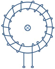
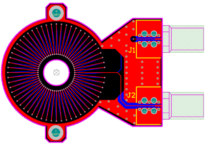
Figure 1 The left diagram shows the Rogowski coil structure, the right diagram shows the PCB Rogowski coil Layout
1.2 Working Principle of Rogowski Coils
Assume an infinitely long current-carrying conductor passes vertically through the center of a Rogowski coil, with conductor current I. The coil inner diameter is a, outer diameter is b, board thickness is h, and the permeability of the PCB trace is μ. As shown in Figure 2.
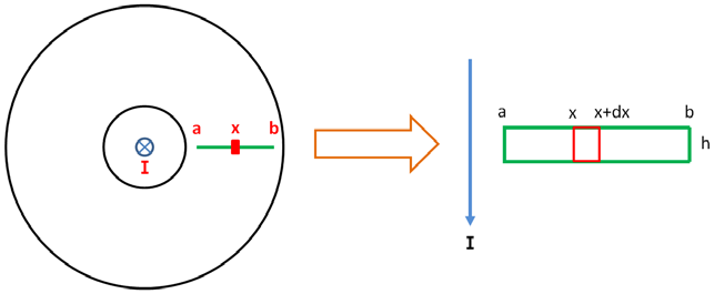
Figure 2 Rogowski coil analysis model, left is top view, right is cross-sectional view
According to the Biot-Savart law, the magnetic flux density at position x:
The top layer trace and bottom layer trace are connected through vias to form 1 turn. The magnetic flux per turn:
According to Lenz’s law, the voltage induced in an N-turn coil:
In equation (3), M is the mutual inductance coefficient.
From equation (3), it can be seen that the output of a Rogowski coil is a voltage that has a differential relationship with the measured current. Therefore, Rogowski coils are only suitable for AC current measurement applications and require an integrator in practice.
1.3 PCB Rogowski Coil Design Considerations
1.3.1 Turn Count Limitation
The main parameter of a Rogowski coil is the mutual inductance coefficient M, whose value is primarily related to the number of turns, board thickness, coil inner diameter, and outer diameter. Among these, limited by PCB via size and manufacturing capabilities, the actual number of turns cannot be infinitely large and has certain limitations. The turn count calculation model is shown in Figure 3.
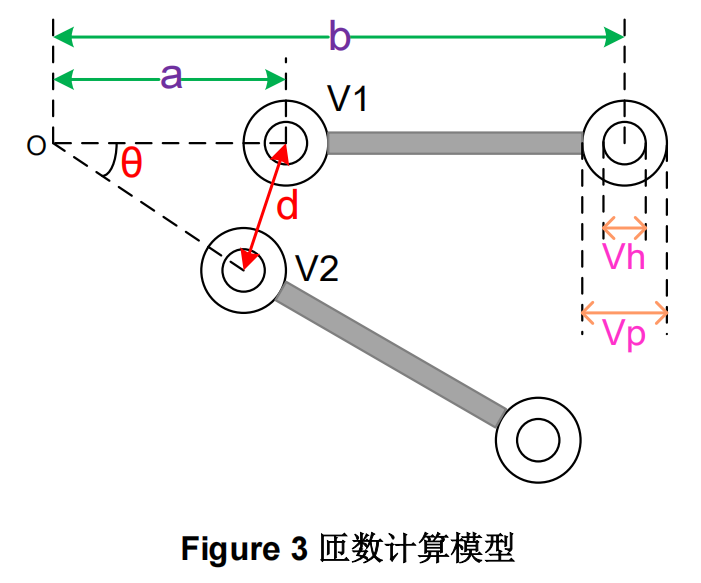
Distance between vias V1 and V2:
Limited by manufacturing capabilities, the distance between these adjacent vias should be at least greater than 3 times the difference between pad and via diameters:
Where V_p is the via pad diameter and V_h is the via diameter.
From equations (4) and (5), the angle between two connected vias can be derived:
Therefore, the maximum number of turns for a PCB Rogowski coil:
Generally, board thickness also determines the minimum via size, so it’s best to confirm with the PCB manufacturer before designing the coil.
1.3.2 Space Utilization
PCB Rogowski coils generally use divergent routing, which creates large gaps between turns in the outer region. Therefore, small turns can be added between large turns to increase the coil’s mutual inductance coefficient without changing the board size, as shown in Figure 4. Let the small turns have inner diameter c and outer diameter d, then the coil’s mutual inductance coefficient:
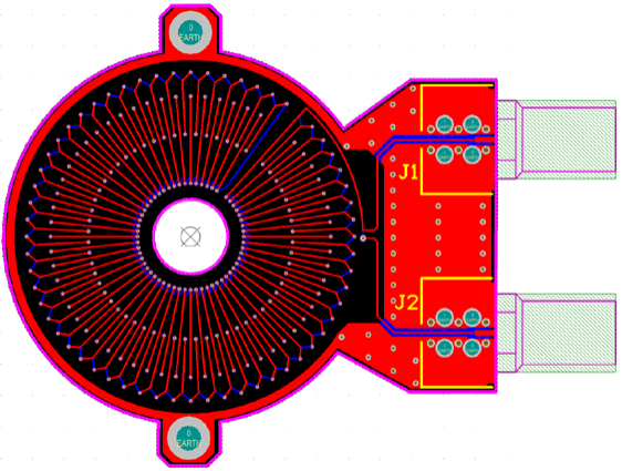
Figure 4 Rogowski coil with added small turns
When a very large mutual inductance coefficient is needed with fixed board size, multiple PCB Rogowski coils can be connected in series end-to-end, i.e., connecting the J2 output of Figure 4 to the J1 of the next PCB coil to achieve signal superposition.
2 Integrator Circuit Design
2.1 Limitations of Ideal Integrator and Improvements
Since the Rogowski coil’s output voltage is the differential of the measured current signal, if there is no integrator circuit in the subsequent stage, even slight high-frequency components in the current will induce high voltage at the coil output, thereby overwhelming the fundamental signal. Therefore, an integrator circuit is needed in the subsequent stage to restore the signal. The ideal integrator circuit is shown in Figure 5.
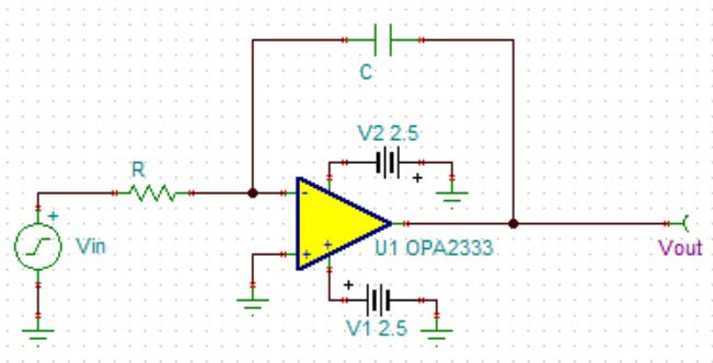
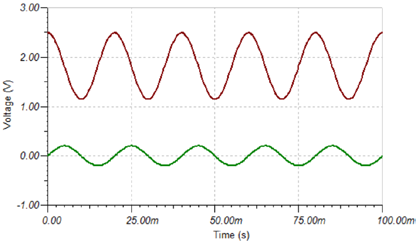
Figure 5 Left shows the ideal integrator circuit schematic, right shows the integrator output voltage waveform
When the input signal offset is zero, the integrated output waveform offset should also be zero. However, as seen above, the integrator output voltage offset is not zero, and the waveform drifts to the power rail. The situation is worse with actual op-amps, as the waveform will clip at the power rail, causing saturation distortion or cutoff distortion. The main reason is that current op-amps are not ideal and have inherent offset voltage. With no other path, the offset charges the integrator capacitor, inevitably leading to capacitor saturation and clipping over time. Therefore, a resistor needs to be connected in parallel with the integrator capacitor to provide a discharge path for the capacitor, enabling stable circuit operation, as shown in Figure 6. After adding the parallel resistor, it is necessary to analyze the circuit’s integration performance.
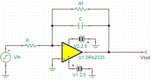
Figure 6 Integrator circuit performance analysis with parallel resistor
At the op-amp’s inverting input, establishing Kirchhoff’s current equation:
Equation (9) is a first-order non-homogeneous equation, whose solution is:
Where C_1 is a constant. Assuming input signal V_{in} = \cos(\omega t), equation (10) can be simplified to:
From a frequency domain perspective, the circuit’s gain magnitude after adding the parallel resistor:
Equations (11) and (12) convey two important pieces of information:
- As time t increases, the exponential term C_1 e^{-\frac{t}{R_f C}} in the output voltage V_{out} gradually becomes smaller and can eventually be completely ignored;
- When R_f \gg \frac{1}{\omega C}, \varphi \approx 0^\circ, and the gain magnitude approaches the ideal \frac{1}{\omega RC}, at which point the output voltage can be considered as the inverted integral of the input signal.
Based on the above analysis, the integrator circuit simulation results are shown in Figure 7. The green curve is the input, and the red curve is the output. The output signal shows fluctuations in the initial stage due to the exponential factor, but eventually stabilizes with excellent integration performance.
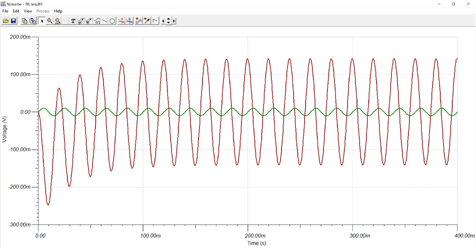
Figure 7 Integrator circuit simulation waveform with parallel resistor
2.2 Op-Amp Selection for Integrator Circuit
To achieve good integration performance, the feedback resistor Rf generally needs to be selected as large as possible, but not excessively large. The main reason is that the integrator circuit acts as a non-inverting amplifier for the op-amp offset. An excessively large feedback resistor Rf will result in a large DC offset at the output, weakening the integrator drift suppression capability. Therefore, the op-amp in the integrator circuit should have a very small offset value to ensure the DC level at the output is as low as possible. OPAx333 is a low-offset op-amp with Zero Drift functionality introduced by TI, which uses internal digital calibration to significantly reduce offset and drift voltage. Its maximum offset is only 10µV, with drift as low as 0.05µV/°C, making it very suitable for integrator circuit design. Figure 8 shows the DC simulation of the OPA2333 integrator circuit. It can be seen that even when the feedback resistor is 1000 times the integrator resistor, the output is only 2.66mV, demonstrating excellent performance. Additionally, OPAx333 has a maximum quiescent current of only 25µA, making it a low-power, high-performance operational amplifier.
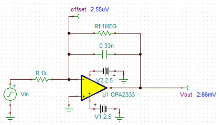
Figure 8 OPA2333 integrator circuit DC simulation
2.3 Single-Supply Integrator Circuit Design
The aforementioned integrator circuit uses a dual-supply integration solution. However, many customer applications only support single-supply operation, making it necessary to design a single-supply integrator circuit. Referencing the differential op-amp circuit structure, the single-supply integrator circuit is designed as shown in Figure 9.
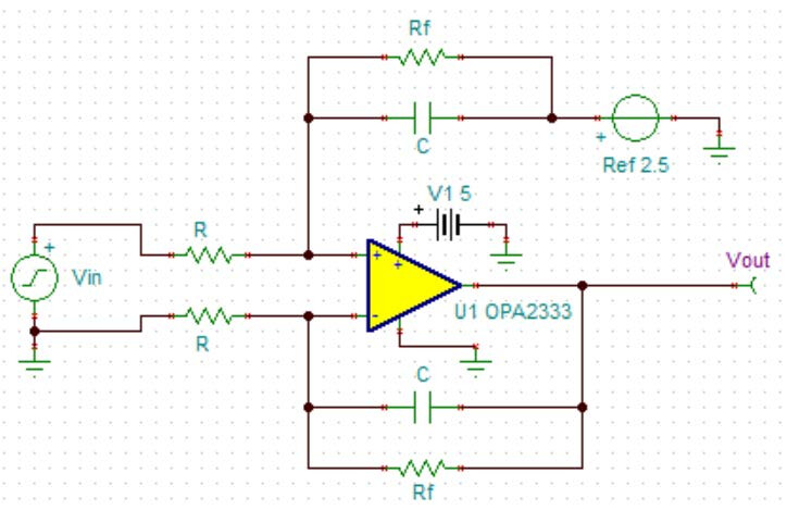
Figure 9 Single-supply integrator circuit
Similar to the previous analysis method, if the input voltage V_{in} = \cos(\omega t), then the output voltage:
Key interpretation of equation (13):
- Output characteristics: The output voltage is the non-inverting integral of the input signal, including a DC offset V_{ref};
- Simulation verification: The simulated output waveform corresponds to Figure 10, where the green curve is the input signal and the red curve is the output signal, showing good system integration performance.
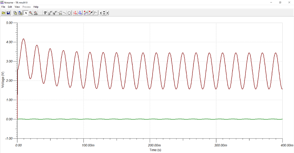
Figure 10 Single-supply integrator circuit simulation waveform
2.4 Considerations for High-Performance Integrator Circuits
2.4.1 Offset Correction
From the previous circuit analysis, the voltage offset at the output has some error, which for OPAx333 op-amps is at most a few mV (while poorer op-amps could reach hundreds of mV). If higher offset requirements are needed at the output, the offset must be corrected. The correction circuit is placed after the integrator circuit, as shown in Figure 11. The simulation results show that the DC offset at output Vout differs from the preset Ref value by only 27µV, demonstrating excellent offset performance. Meanwhile, the non-inverting gain resistors R2 and R3 can further condition the signal to achieve full swing.
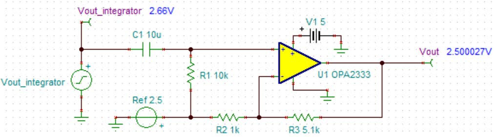
Figure 11 Offset correction circuit and DC simulation results
2.4.2 Measurement of High-Frequency Fault Components
In some applications (such as AFCI), users are primarily concerned with the high-frequency fault components of current to take appropriate actions (such as circuit interruption) under fault conditions. In these cases, the low-frequency normal operating current is less important and can even be ignored. For this application scenario, a high-pass filter can be set up first to filter out low-frequency components. Then an amplifier circuit can be added to amplify the high-frequency components, ensuring the integrated signal is sufficient to be monitored. The application circuit is shown in Figure 12.
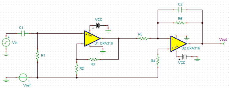
Figure 12 High-frequency fault component measurement circuit
2.4.3 Low-Frequency Phase Correction
From the previous analysis, the integrator circuit has some phase angle error, which is larger at lower frequencies. Taking the circuit in Figure 8 as an example, at a 50Hz operating frequency, the simulation waveform results are shown in Figure 13. The green curve is the input, and the red curve is the integrator output.
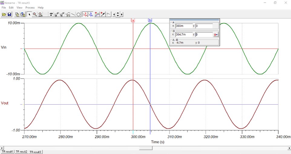
Figure 13 Inverting integrator circuit simulation waveform phase analysis
Theoretically, for a 50Hz sine signal undergoing inverting integration, the zero-crossing point of the integrated waveform should lag the input signal by 90°, which in the time domain means point b lags point a by 5ms. However, as seen in Figure 13, the time difference between points a and b is 4.7ms, which converts to approximately 84.6° in phase angle. This means the integrator output waveform leads the expected design by about 5.4° in phase angle. Phase correction generally needs to be considered in two scenarios: First, when the system has high phase accuracy requirements, such as controlling circuit breaker switching, where inaccurate phase can generate large arcs, threatening equipment and personal safety; Second, when the system operates at low frequencies, such as for power utilities where power frequency (50/60 Hz) is the main application, low frequency brings larger phase angle errors.
Below is the analysis of the phase angle error generation mechanism and correction measures. The integrator circuit’s phase angle error:
If an offset correction circuit is used, it will generate another phase angle error:
Both \varphi_1 and \varphi_2 generate leading phase angles, so a lag compensation stage is needed to cancel them out, as shown in Figure 14. Phase correction is mainly divided into active and passive types. Active correction provides the best results and is not affected by load impedance, but requires an additional op-amp, resulting in higher cost; passive correction has very low cost, but its correction effect is affected by load impedance. The choice depends on application requirements. To ensure good correction performance, capacitors in the integrator circuit and low-frequency correction circuit should preferably be C0G or NP0 series.
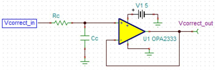
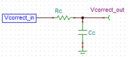
Figure 14 Left shows active phase correction, right shows passive phase correction
3 System Testing
3.1 Performance Testing
Taking a 50Hz power frequency application as an example, a single-supply integrator circuit is designed as shown in Figure 15. The expected design goal is that the output voltage varies linearly with input current with a proportionality coefficient of 52.4. The Rogowski coil design parameter is 101nH.
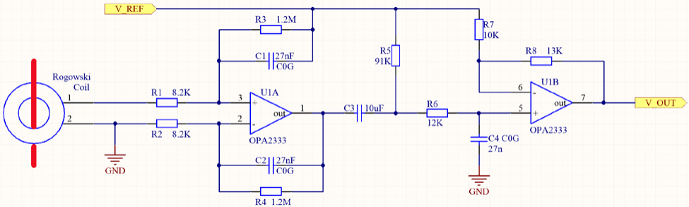
Figure 15 Single-supply integrator circuit schematic for power frequency application
The current conductor is passed vertically through the PCB Rogowski coil. Limited by the measurement equipment’s output current capability, the number of turns was increased. The test environment and waveforms are shown in Figure 16.
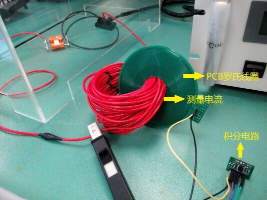
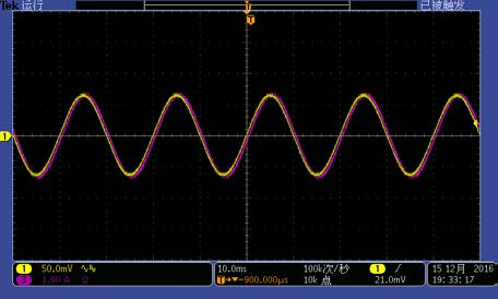
Figure 16 Left shows test environment, right shows measurement waveform (purple trace is current, yellow trace is integrator output voltage)
As seen in the right side of Figure 16, the output voltage waveform basically matches the current waveform, achieving good measurement results. The measurement data is compiled in Table 1.
Table 1 PCB Rogowski Coil Measurement Data
| Input Current (RMS)/A | Output Voltage (RMS)/mV | Input Current (RMS)/A | Output Voltage (RMS)/mV |
|---|---|---|---|
| 0.46 | 20.95 | 2.74 | 124.8 |
| 0.92 | 42.03 | 3.26 | 148.0 |
| 1.39 | 63.02 | 3.68 | 166.8 |
| 1.83 | 83.70 | 4.01 | 185.4 |
| 2.30 | 104.6 | 4.46 | 202.5 |
The data from Table 1 is linearly fitted, as shown in Figure 17. The results show that the linearity between output voltage and input current is very good, approximately satisfying the following relationship:
According to theoretical calculations, the relationship between output voltage and input current is:
The measured coefficient 45.64 is slightly smaller than the theoretical result of 47.21, but the error is controlled within 5%, basically meeting the expected design target.
3.2 Performance Test Error Analysis and ImprovementTest errors are mainly related to the relative position between the current-carrying conductor and the coil. To reduce errors, it is generally required that a longer current-carrying conductor passes vertically through the center of the Rogowski coil, and wire bending should be minimized as much as possible. Due to the limitation of small measured current in this test, the method of increasing the number of turns was adopted to improve the coil’s equivalent mutual inductance coefficient. Therefore, the current-carrying conductor did not completely pass through the coil center, and there was significant cable bending. Consequently, the measured coil mutual inductance coefficient was smaller than the theoretical value, but the difference was not significant, basically matching the design target.
3.3 Interference Testing
When measuring current with a Rogowski coil, the measured current is required to pass through the center hole of the coil. However, in actual working environments, there are generally other alternating currents around the measured current (such as in three-phase AC transmission scenarios). According to the working principle of the Rogowski coil, peripheral alternating currents can also generate alternating magnetic fields in the coil, interfering with the measured current. Therefore, analyzing the anti-interference capability of the Rogowski coil against surrounding currents becomes necessary.
The basic process of interference testing is to first measure the correspondence between output voltage and measured current without interference current. Then, interference current is added around the measured current (i.e., outside the coil) to verify whether the integrated output voltage changes under the same measured current. Based on this concept, the measurement environment for Rogowski coil interference testing is shown in Figure 18.
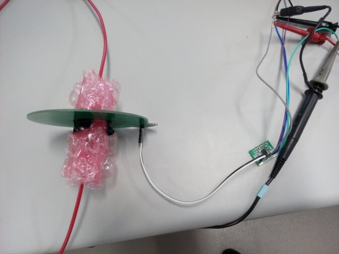
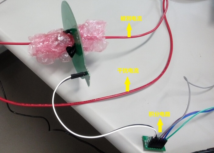
Figure 18 The left image shows the measurement environment without interference current, the right image shows the measurement environment with interference current
Limited by the inability to provide large interference current at the test site, to achieve better interference effects, the measured current did not have increased turns, and the interference current was made comparable in magnitude to the measured current. As compensation for the turns, the amplification factor of the integrator circuit was increased in the interference testing (R7 in Figure 15 was changed to 100Ω). It should be noted that an excessively large amplification factor brings some disadvantages, such as increased output offset, and increased deviation between the actual gain and design value of the amplification factor. Therefore, a large amplification factor should not be selected in practical applications. However, in this anti-interference testing, we are more concerned about the impact of interference signals on measured signals with a fixed circuit, so the impact of larger gain is not significant.
The integrated output voltage waveforms measured with and without interference current are shown in Figure 19.
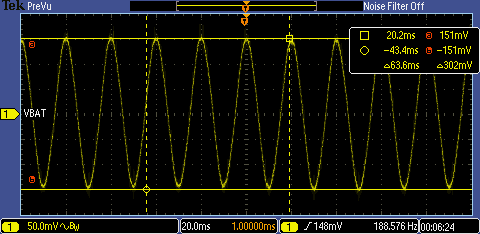
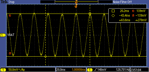
Figure 19 The left image shows the output voltage waveform without interference current, the right image shows the output voltage waveform with interference current
The test data is further organized as shown in Table 2.
Table 2 Interference test data
| Measured current (RMS)/A | Interference current (RMS)/A | Output voltage without interference current (RMS)/mV | Output voltage without interference current (RMS)/mV | Error% |
|---|---|---|---|---|
| 0.41 | 0.41 | 21.9 | 20.6 | -5.9% |
| 0.82 | 0.81 | 43.1 | 38.9 | -9.7% |
| 1.23 | 1.22 | 65.1 | 58.5 | -10.1% |
| 1.64 | 1.63 | 83.4 | 78.5 | -5.9% |
| 2.06 | 2.04 | 106.1 | 98.3 | -7.4% |
As can be seen from Table 2, the introduction of interference current reduces the amplitude of the output voltage, causing measurement errors. In this test, the error is around 10%.
3.4 Interference Test Error Analysis and Improvement
When interference current exists outside the Rogowski coil, the changing interference current generates an alternating magnetic field, which induces an electromotive force in the Rogowski coil. This is the fundamental cause of measurement errors. The magnitude of measurement error is related to the interference current value and also to the distance between the interference current and the measured current. In this test, the interference signal was very large, comparable in magnitude to the measured signal, and the distance between the interference signal and the Rogowski coil was short, thus causing relatively large measurement errors. In actual measurement, care should be taken to keep interference current away from the Rogowski coil, and reduce interference current when conditions permit, thereby reducing measurement errors.
4 References
- TI-Design-01063, High Accuracy AC Current Measurement Reference Design Using PCB Rogowski Coil Sensor, Texas Instruments Inc.
- OPA2333 datasheet 2016, Texas Instruments Inc.