INA226 Measurement Offset/Nonlinearity Problems

Hello everyone, I’m building a DIY battery tester / electronic load using an ESP32, TFT display, and some other interesting components. The core of this project is a current sink with a feedback loop, featuring a digitally controlled setpoint. While I have some ideas for design improvements (I admit I made a few questionable choices), the most frustrating issue right now is with the INA226 current measurement.

Problem Description:

When the input voltage at the PCB terminals is low (for example, around 4V), I try to increase the current and find that the INA226 readings are lower than the actual current (verified with a digital multimeter), and the error is non-linear. As the set current increases, this deviation becomes more pronounced.

  • The issue appears when current exceeds approximately 50mA;
  • When the input voltage is higher (around 18V), the problem nearly disappears;
  • Interestingly, the feedback loop setpoint matches the actual current very closely — typically within ±0.5mA error.

So essentially, my load is working as expected, but the INA226 seems to “under-report” current values at low voltage.

Questions:

  1. Has anyone encountered this behavior with the INA226 under load at low bus voltage?
  2. Could this be related to shunt voltage drop, I2C timing, or other factors?
  3. What suggestions are there for stable readings or improving measurement accuracy in this scenario?

If further information is needed, I can share more photos, wiring diagrams, code snippets, or the complete KiCad project files. Thank you very much for any guidance or similar experience sharing!

Have you considered the stability issues that may arise from the interaction between C1 and R4? This would introduce delay to the inverting input of the op-amp, and combined with the delay introduced by the Darlington transistor, may be sufficient to cause oscillation or some form of ringing.

I admit I hadn’t considered that before. My thinking was that since the battery voltage is stable, fast adjustment isn’t needed, and using an RC low-pass filter can reduce noise/oscillation. I’ll definitely check this with an oscilloscope.

Also, I forgot to mention that Q1 has already been changed from 2N2222 to BD139.

The RC low-pass filter (C1 and R4) in your feedback loop might be the culprit, as mentioned in the reply. At low input voltages, the loop delay (from RC and Darlington transistor Q1) could cause phase shifts, leading to unstable current regulation and thus distorted INA226 readings. Try reducing the RC time constant—use a smaller capacitor C1 (e.g., from 100nF to 10nF) or resistor R4—to speed up the feedback response. Also, since you replaced Q1 with BD139, ensure its base drive is sufficient; insufficient drive can cause the transistor to operate in the linear region, increasing current nonlinearity. Use an oscilloscope to observe the shunt voltage waveform—if there’s ringing or oscillation, adding a small snubber capacitor (e.g., 10pF) across the shunt resistor might help stabilize the signal.

Let’s break down the phenomenon:

  1. The current loop itself is fine (setpoint ≈ measured value), indicating the closed loop with MOSFET, op-amp, and DAC is working properly;

  2. Only the INA226’s “reported value” is low, and it specifically occurs when VBUS is low and current is high;

  3. At 18 V, almost no error is visible.

This almost points directly to device-level measurement errors caused by “too low common-mode voltage across the shunt resistor,” rather than code or I²C timing.

  1. Common-mode too low, internal PGA starts to underperform
    INA226’s input stage is a ΔΣ-type ADC with a 2 MHz switched-capacitor array at the front end. The lower the common-mode voltage, the more pronounced the charge injection mismatch in the internal sample-and-hold, amplifying the equivalent offset. The datasheet clearly states: when VCM = 0 V, typical offset is 50 µV, dropping to the 10 µV range when VCM ≥ 1 V. With your 4 V input and 50 mA current, assuming a 50 mΩ shunt resistor, VBUS is actually pulled down to 4 V – 2.5 mV ≈ 3.9975 V, which is still considered “low” for common-mode. More critically, the shunt voltage is only 2.5 mV, already the same order of magnitude as the offset voltage; as current increases further, the readings start to lose accuracy.

  2. Kelvin routing/pad thermocouple effects of the shunt resistor
    At low voltage and high current, an additional 1 µΩ of metal resistance introduces a 1 µV error. If the top-layer copper is etched away significantly, or the sampling points are too far from the pads, the actual Vshunt reaching the INA226 will be lower than what the multimeter measures.

  3. On-board ground bounce
    If power ground, digital ground, and INA226’s GND share a thin trace, 50 mA switching spikes can create ground differences of several hundred µV, directly superimposing on the differential measurement.

  4. I²C timing/noise
    Such errors typically manifest as “jitter” or “code flickering” rather than systematic low readings, so this should be lower priority.

Improvement checklist (sorted by cost-effectiveness)

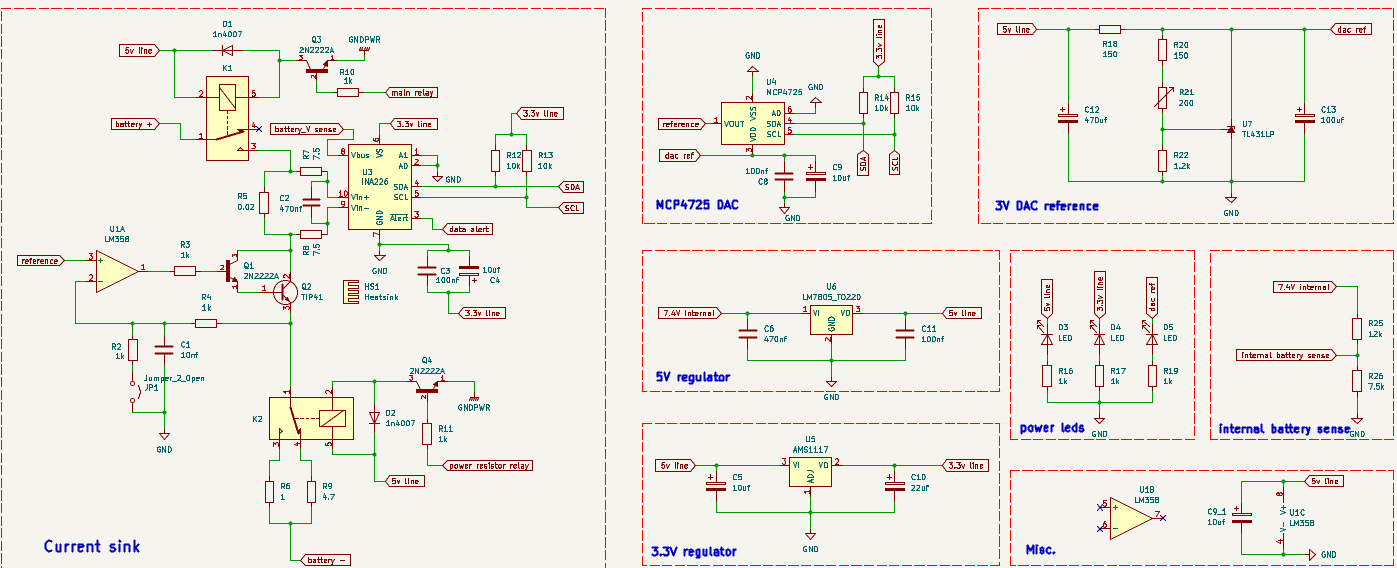
A. Move the shunt resistor to the “high side”
Let INA226’s VBUS pin sit directly on the battery positive terminal, so common-mode ≈ 4 V, far above the 1 V “comfort zone,” immediately reducing device offset by an order of magnitude. High-side measurement requires:
– Move the shunt resistor to the positive side;
– INA226’s V+ supply can be 3.3 V, since common-mode is allowed up to 36 V;
– Note that new traces must be Kelvin and separated from the power path.

B. Increase the shunt voltage
If the maximum current is 1 A, replace the 50 mΩ with 100 mΩ, giving a full-scale of 100 mV. The LSB remains 2.5 µV, but the signal-to-offset ratio doubles. Power dissipation is 100 mW, which is acceptable for a 1 A application.

C. Calibrate the “zero offset”
Perform a “zero-current” sampling in code (relay disconnected or DAC=0), store the result in EEPROM, and subtract it before each formal test. The INA226 itself has a Calibration register, but that only works for power/current calculations, not for raw shunt voltage; so directly reading the Shunt Voltage Register and subtracting the offset is the cleanest approach.

D. Minor board rework
– Partition power ground and digital ground, connect at a single point;
– Use the entire layer under INA226 as “analog ground” copper, meeting power ground only at a single point through a 0 Ω resistor or pin header;
– Place two pairs of Kelvin vias inside the shunt resistor pads, run differential traces parallel in inner layers, length <15 mm.

E. Software filtering
Collect 64 samples for averaging, then smooth the result with a second-order IIR filter, which can suppress random noise below 0.2 LSB. However, this is ineffective against systematic offset and should only be used in conjunction with A/B/C.

Quick verification methods

  1. Temporarily use a lab power supply in series with a 1 Ω resistor to artificially raise VBUS above 8 V, and see if the error immediately decreases;

  2. Use a precision millivolt source (or DAC+voltage divider) to inject 1 mV, 5 mV, 10 mV directly into INA226’s differential pins, read the Shunt Voltage Register, and plot the “input-code” curve to immediately see the device’s linear region.

Typically, after completing items A+B+C, you can suppress the error at the 4 V/1 A point to within ±0.5 %FS. The rest is just a software calibration issue. Good luck with debugging!

Based on your description, the issue of INA226 showing lower-than-actual and nonlinear current readings at low input voltages (e.g., 4V) with large currents, while the problem disappears at high voltages (18V), can be analyzed and addressed as follows:

1. Common-Mode Voltage and Shunt Voltage Drop

The common-mode voltage range of INA226 is critical. It requires V- ≤ VCM ≤ V+ (where V- is ground and V+ is typically the bus voltage). However, the voltage drop across the shunt resistor (I×Rshunt) alters the sampling voltage. When the input voltage is low (e.g., 4V), increasing the current causes the common-mode voltage at the sampling terminal to approach or drop below the minimum common-mode operating voltage of INA226, leading to reduced measurement accuracy and nonlinearity.

For example, if your shunt resistor is 0.02Ω (inferred from R5=0.02Ω in the schematic), the voltage drop is 10mV at 500mA. With a 4V bus voltage, the common-mode voltage at the sampling point decreases due to this drop, approaching the lower limit of INA226’s common-mode range, thus causing measurement deviations. At 18V, the shunt drop is negligible, so the common-mode voltage stays within the normal range.

2. Shunt Resistor Power Dissipation and Temperature Drift

The shunt resistor heats up under large currents, leading to resistance change with temperature (temperature drift), which causes nonlinear measurements. Especially at low voltages and large currents, the power dissipation (I²×R) of the shunt resistor is significant, resulting in noticeable temperature rise and resistance variation, making the current value calculated from the sampling voltage deviate from the actual value.

3. I2C Timing and Communication Stability

Although the feedback loop works normally, the I2C communication of INA226 may have timing deviations under low voltage supply. Check if the supply voltage of INA226 (3.3V from AMS1117 in the schematic) is stable at low bus voltages. Additionally, the pull-up resistors of I2C and the communication speed (e.g., exceeding the device’s supported rate) can also affect the accuracy of data reading, leading to reading deviations.

4. Circuit Layout and Noise Interference

Parasitic inductance or resistance in the wiring of the shunt resistor, or crosstalk with other high-frequency circuits (such as TFT display and ESP32’s high-frequency signals), can also affect sampling accuracy. Especially in low-voltage and small-signal scenarios, the impact of noise is amplified.

Suggestions for Stable Reading and Improved Accuracy

  • Common-Mode Voltage Optimization: Ensure the common-mode voltage of INA226 is always within its specification range. Try adjusting the shunt resistor value (e.g., choosing a smaller resistance to reduce voltage drop, while balancing power and resolution) or limit the maximum current in low-voltage scenarios to avoid excessively low common-mode voltage.
  • Shunt Resistor Selection: Use low-temperature-coefficient alloy resistors (such as manganin alloy) and ensure sufficient power margin (at least twice the actual power consumption) to reduce the impact of temperature drift. Meanwhile, optimize the heat dissipation design of the shunt resistor, such as increasing thermal pads or copper areas.
  • I2C Communication Optimization: Reduce the I2C communication speed (e.g., from 400kHz to 100kHz), check if the pull-up resistor value matches (typically around 4.7kΩ for 3.3V systems), and ensure the I2C timing between ESP32 and INA226 strictly complies with the device manual. You can also add decoupling capacitors (such as paralleling 10μF and 0.1μF capacitors at the V+ pin of INA226) to improve supply stability.
  • Circuit Layout Improvement: Keep the sampling lines of the shunt resistor as short and thick as possible to reduce parasitic parameters; place INA226 away from high-frequency interference sources (such as TFT display driver circuits), and shield the sampling lines or use single-point grounding if necessary.
  • Software Calibration and Compensation: Establish a calibration table for low-voltage scenarios in the code, and compensate the INA226 readings based on input voltage and set current. For example, measure the deviation at different voltages and currents with a digital multimeter, fit a compensation function, and correct it in real time in the software.