I’d like to ask you experts a question. I’m generating a PWM signal using an STM32G474 and sending it to the UCC21520AQDWRQ1 to drive MOSFETs. The problem is that I’m inputting a pair of equal and opposite square waves into the UCC21520AQDWRQ1 (verified correct with an oscilloscope). However, regardless of whether I connect the subsequent MOSFET stage or not, only OUTB (lower switch) on the output side of the UCC21520AQDWRQ1 shows the amplified square wave (measured with one oscilloscope probe lead connected to GND and the other to OUTB). OUTA (upper switch) shows nothing—though there seems to be some noise-like signal when measuring between OUTA and VSSA. When the MOSFETs are not connected, the voltage between VDDA and VSSA is 0V; once they’re connected, this rises to about 4.3V. I’ve also tried connecting VSSA to ground and then measuring the waveform at OUTA, but still see nothing.
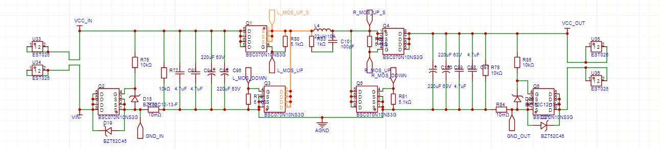
The UCC21520 is an isolated driver, and both output channels must be connected to independent power supplies. The lower MOSFET must be soldered in place—only then can the ground (VSSA) of Channel A connect to your system GND through the lower MOSFET when it’s turned on, forming a closed loop to charge the bootstrap capacitor for the high-side MOSFET. Then, when the lower MOSFET turns off and the upper MOSFET turns on, the high-side driver is powered via the bootstrap capacitor (note: the oscilloscope ground must be connected to VSSA).
Additionally, the two channels (A and B) must receive complementary PWM signals, and dead-time must be properly set.
Alright, I’ll go try it out
This is a classic issue encountered when working with “Half-Bridge” or “High-Side” gate drivers like the UCC21520. Based on your description and schematic, here is an analysis of why your High-Side (OUTA) is not working and how to fix it.
1. The “Disconnected” Behavior (0V) is Normal
You mentioned that when the MOSFETs are not connected, the voltage between VDDA and VSSA is 0V. This is completely normal for a bootstrap-powered circuit.
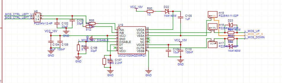
- The high-side power (VDDA) is supplied via the “Bootstrap” capacitor (C108).
- This capacitor can only charge when the switching node (VSSA / L_MOS_UP_S) is pulled to Ground.
- When the MOSFETs are disconnected, VSSA is floating. There is no path for current to flow from VCC_10V through the diode (D22) to charge C108. Therefore, the high-side driver has no power and will not output anything.
2. The 4.3V Problem (UVLO)
Once you connect the MOSFETs, you see the voltage rise to 4.3V. This is the core of your problem.
- UVLO (Under-Voltage Lock-Out): The UCC21520 has an internal protection circuit. For the
AQDWRQ1version, the UVLO threshold for the output channels is typically around 8V (rising) and 7.3V (falling). - If the voltage between VDDA and VSSA is only 4.3V, the high-side driver stays in “Lock-out” mode to prevent damaging the MOSFET with insufficient gate voltage. This is why OUTA shows nothing.
Why is it only 4.3V?
- Check your VCC_10V rail: Measure the voltage at the anode of D22 relative to GND. Is it actually 10V? If that rail is actually 5V, then 5V minus the diode drop (~0.7V) equals exactly 4.3V.
- Bootstrap Refresh: For the bootstrap capacitor to charge to the full rail voltage, the low-side MOSFET (Q3) must turn ON for a sufficient amount of time. If your PWM duty cycle for the low-side is extremely small, or if you aren’t switching the low-side at all, the capacitor won’t charge properly.
- Diode Speed: You are using a 1N4148W. While fast, it has a relatively high forward voltage drop and limited current. For power stages, it is usually better to use a Fast Recovery Diode or a Schottky diode with a high enough voltage rating (e.g., RS1M or similar).
3. Measurement Technique
You mentioned seeing “noise-like signals” when measuring OUTA to VSSA.
- Floating Reference: Remember that VSSA is the “Switching Node.” It jumps from 0V to VCC_IN (e.g., 24V or 48V) every cycle.
- If you connect a standard oscilloscope probe ground clip to VSSA, you are connecting the scope’s chassis ground to a high-speed switching node. This creates massive common-mode noise and can even blow up your scope or the driver.
- To measure correctly: Use a Differential Probe, or use two probes (Channel 1 on OUTA, Channel 2 on VSSA) and use the Math function (CH1 - CH2).
Recommended Steps to Fix:
- Verify VCC_10V: Ensure the supply entering the driver stage is actually 10V-12V. If it’s 5V, the UCC21520 high-side will never start.
- Initial Power-Up Sequence: In your STM32 code, ensure you pulse the Low-Side (INB) a few times before starting the High-Side (INA). This “primes” the bootstrap capacitor.
- Check Minimum Duty Cycle: Ensure your PWM frequency isn’t so high that the dead-time or low-side “on-time” is too short to charge the 1uF capacitor (C108).
- Hardware Check: Ensure the connection at header H16 (VSSA to Source) is solid. If there is high resistance here, the bootstrap charging will fail.
- Test with a fixed supply: To rule out bootstrap issues, you can temporarily connect an external isolated 10V power supply directly across C108 (Positive to VDDA, Negative to VSSA). If OUTA starts working, you know the issue is purely with your bootstrap charging logic or voltage levels.
Can this chip achieve 100% duty cycle if two isolated power supply modules are used to power VDDA and VDDB separately?
Yes, it is possible. By using two isolated power supply modules to independently power the VDDA and VDDB of the UCC21520, 100% duty cycle operation can be fully achieved. This is one of the standard design approaches for this chip in high-side/low-side driving configurations.
Core Principles and Rationale
-
Official Design Support: The UCC21520 is a dual-channel isolated gate driver with independent secondary-side power domains A and B (VDDA/VSSA, VDDB/VSSB), supporting separate power supplies for each channel. The datasheet explicitly states that it can be configured for dual high-side, dual low-side, or half-bridge driving, making it fully compatible with independent power supply architectures.
-
Key Difference from Bootstrap Solutions:
- Bootstrap circuits cannot sustain 100% duty cycle operation, because the bootstrap capacitor must recharge during low-side conduction, limiting high-side duty cycle.
- Independent isolated power supplies have no such limitation—each channel is powered separately, enabling stable continuous adjustment from 0% to 100% duty cycle.
-
Hardware Isolation Assurance: There is 1500 VDC internal functional isolation between the two secondary-side power domains, allowing tolerance of high common-mode voltages and ensuring reliability and signal integrity when high-side and low-side channels operate simultaneously.
Key Design Considerations
-
Power Supply Selection: The VDDA/VDDB supply range is 3 V–18 V. It is recommended to use isolated power modules with low output ripple and fast transient response to meet gate drive requirements.
-
Decoupling Capacitors: Place low-ESR/ESL ceramic capacitors (recommended 0.1 µF–1 µF) close to each power rail, directly adjacent to the VDDA-VSSA and VDDB-VSSB pins, to minimize parasitic inductance and noise interference.
-
Grounding and Layout: The grounds of the two power supplies (VSSA and VSSB) should be connected at a single point to avoid ground loops. Maintain symmetrical PCB layout to optimize drive loops and reduce EMI and switching noise.
-
Input Control: Configure the INA/INB inputs correctly to prevent unintended triggering of the dead-time circuitry and ensure independent channel control.
Practical Application Verification
TI’s official forum includes cases where engineers successfully achieved 100% duty cycle output in inverters by powering VDDA and VDDB with two independent 12 V isolated power supplies, confirming the feasibility and stability of this approach.
Summary
By powering VDDA and VDDB with independent isolated power supplies, the UCC21520 can achieve 100% duty cycle without limitations, making it an optimal solution for high-side/low-side, full-bridge, and similar topologies—completely avoiding the duty cycle constraints inherent in bootstrap circuits.