Design concept:
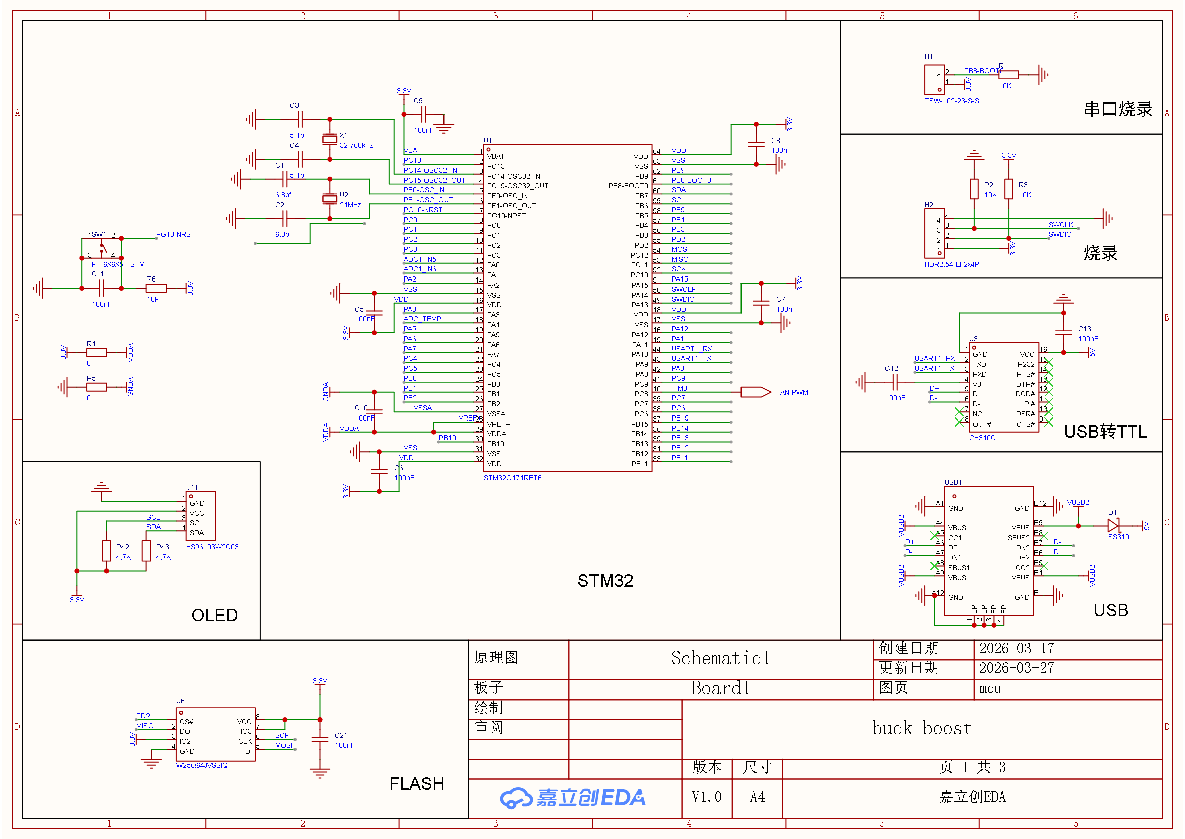
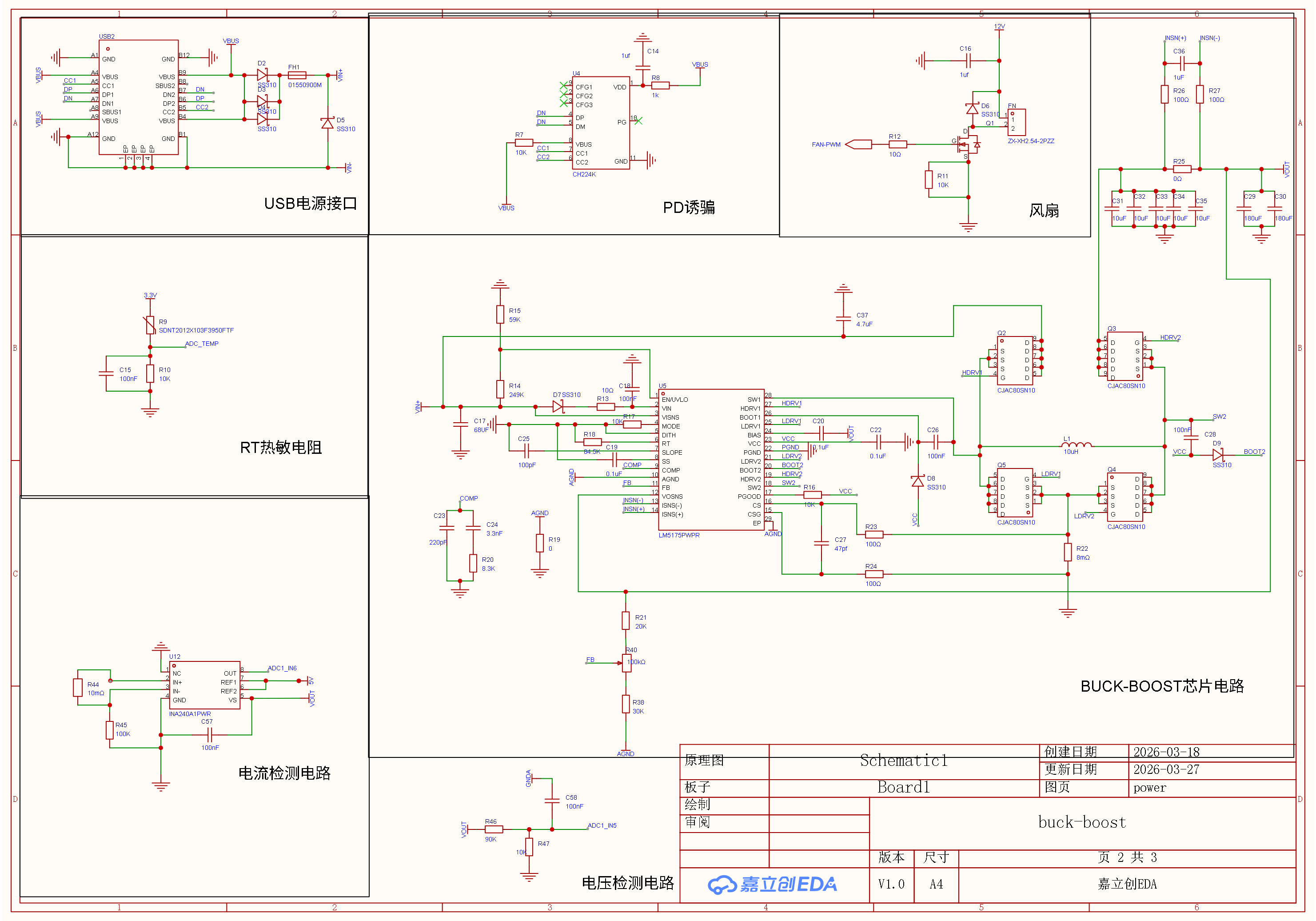
Input 20V via USB, then step down to an output voltage of 5–30V using the LM5175PWPR (output regulated by adjusting the feedback network via potentiometer R40). The current and voltage sensing circuits feed data to the STM32’s ADC pins. The MCU processes this data and displays the values on an OLED screen. A thermistor measures temperature and adjusts the fan speed via PWM control.
Questions:
Are the current and voltage sensing circuits properly designed?
Is the LM5175PWPR design appropriate (including component selection and circuit configuration)?
Are you converting my open-source buck-boost digital power supply project into a regular analog-controlled buck-boost power supply, using the microcontroller only for current and voltage sampling?
If so, then using an STM32G474 would be somewhat wasteful.
Welcome to the pit! As the senior zeruns mentioned above, using the STM32G474—a “god-tier” MCU renowned for its high-precision timers and mixed-signal capabilities—for a purely analog feedback auxiliary display is definitely “using a cannon to kill a mosquito” . But since this is a beginner’s learning project, having some hardware resource headroom isn’t a bad thing at all. Plus, this board has solid foundations; once you level up later, you can directly build upon it to explore fully digital power supplies (digital loop control), without needing to redesign the PCB.
Here’s my quick take on your two questions:
1. Are the current and voltage sensing circuits reasonable?
Voltage Sensing: Very standard and well-designed. You’re using a 90K (R46) and 10K (R47) resistor divider, giving a 1:10 voltage division ratio. With a maximum output of 30V, the divided voltage going into the MCU is 3V—just within the safe 3.3V ADC range of the STM32. Perfectly reasonable.
Optimization Suggestion: The filter capacitor C35 (100pF) placed across the ADC pin seems a bit small for low-frequency sampling. Consider increasing it to 1nF or even 10nF. Combined with software-based moving average filtering in the MCU, this will greatly stabilize the voltage reading on the OLED, preventing wild fluctuations.
Current Sensing: Using the INA280—a dedicated high-common-mode current sense amplifier—is a robust choice, much more reliable and hassle-free than building one from discrete op-amps.
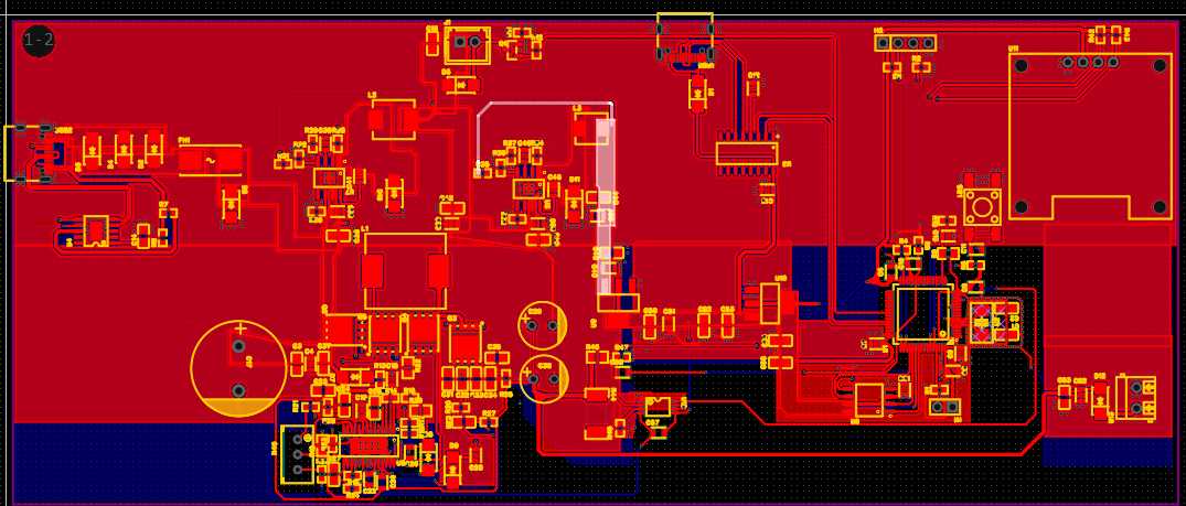
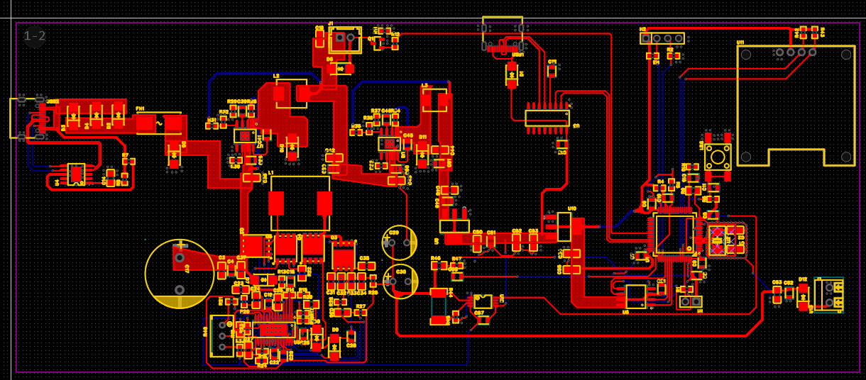
Pitfall Alert: While the schematic looks fine, pay close attention during PCB Layout! The traces connecting the sense resistor (R44 on the schematic) to the INA280 inputs must strictly use Kelvin connections (Kelvin sensing). That means routing differential traces from the inner sides of the sense resistor pads directly to the chip. Do not just connect them via wide copper pours to the power ground plane. Otherwise, the voltage drop across the ground plane caused by high currents will introduce massive errors in your readings.
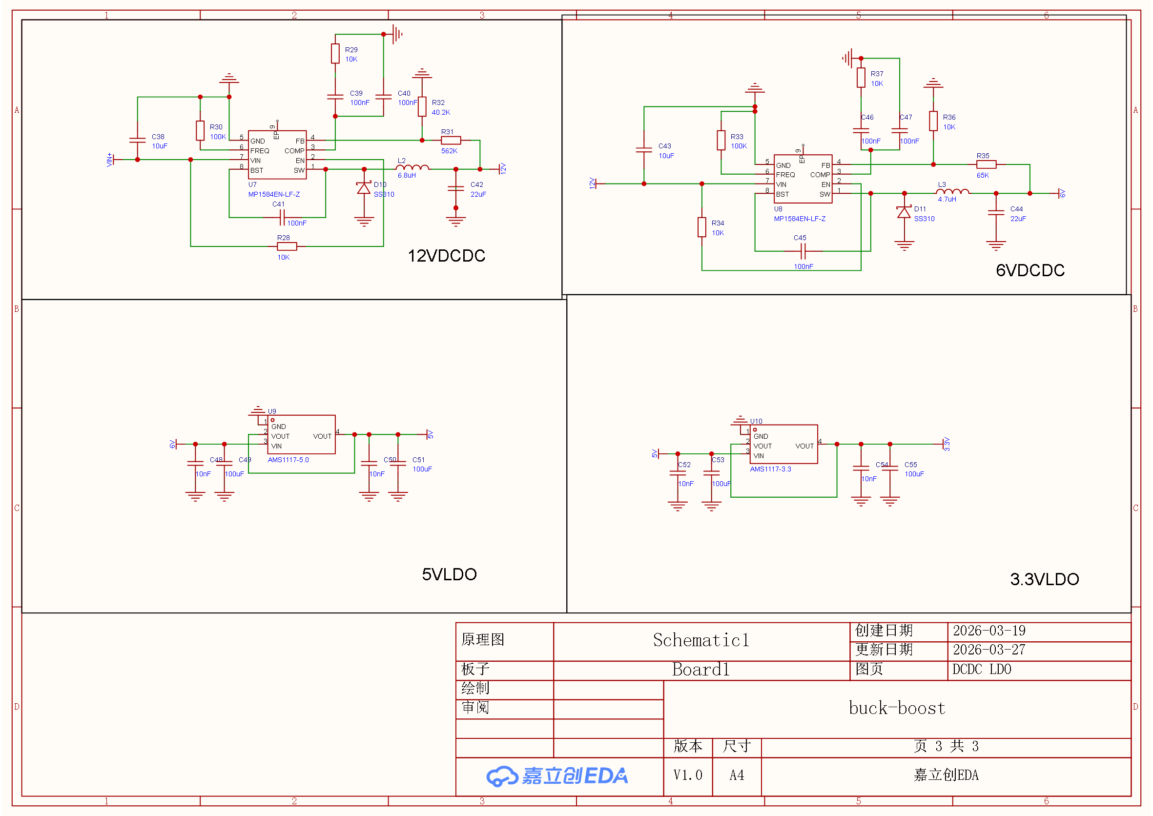
2. Is the LM5175PWPR design reasonable?
Overall architecture appears to follow proven reference designs. The external component values and MOSFET selections should handle a typical 5–30V output without issues.
Regarding Potentiometer-Based Voltage Adjustment (High-Risk Warning): You mentioned using potentiometer R40 to adjust the feedback network. In switch-mode power supplies, directly connecting a mechanical potentiometer to the FB (feedback) pin carries risks. Over time, or during rotation, mechanical pots are prone to momentary contact interruptions (open circuit).
Fortunately, your configuration—where R40 is in series with R38 as the lower feedback resistor to ground—is relatively safe. If R40 momentarily loses contact and opens, the FB pin gets pulled up to the full output voltage, causing the LM5175 to immediately shut down the output, bringing voltage to zero.
(FYI: Had the pot been placed in the upper leg of the divider, a contact failure would pull FB to zero, making the chip think there’s no output. It would then max out the duty cycle instantly, sending your output voltage to dangerous levels—likely frying your load device.)
Layout Is Where the Real Challenge Lies: Controllers like the LM5175, a 4-switch synchronous buck-boost, are extremely sensitive to PCB layout. Getting the schematic right only accounts for about 30% of success. Keep the power loop area as small as possible. Place input/output filter capacitors as close as feasible to both pairs of MOSFETs. Also, ensure that the current-sense resistor traces connected to the LM5175 are routed as matched-length differential pairs.
In summary: As an entry-level learning project, your thinking is clear and your schematics are neat and well-organized. Go ahead and fabricate the board. First, get the analog control loop working, build up some hands-on DC-DC hardware debugging experience, and later you can gradually unlock the full potential of this G474 chip. Good luck—and looking forward to seeing your board light up!
Hello expert, I’ve finished my PCB layout. Could you please help me check if there are any issues? I’m especially unsure about how to properly separate the analog ground, power ground, and digital ground. I’d really appreciate your guidance