“Op-amps aren’t hard; what’s hard is that no one explains them clearly the first time you encounter them.” — A senior who once struggled with op-amps
 Table of Contents
- What Is an Operational Amplifier?
- The Op-Amp Family Tree: More Than Just One Type
- Open-Loop Use: When an Op-Amp Becomes a Comparator
- Introducing Negative Feedback: From Wild Horse to Tamed Steed
- Voltage Follower: The Most Basic and Practical Circuit
- Non-Inverting Amplifier: Signal Direction Preserved, How Much Gain Do You Want?
- Inverting Amplifier: Signal Flipped 180°, Yet Amplified
- Virtual Short and Virtual Open: The “Ren and Du Meridians” of Op-Amp Analysis
 Common Beginner Mistakes (Pitfall Avoidance Guide)
 Quick Reference for Op-Amp Selection: Which Op-Amp for Which Scenario?
 Key Parameter Explained
 Hands-on Experiment: Build Your First Op-Amp Circuit on a Breadboard
- Appendix: Quick Reference Table of Classic Op-Amp Models
1. What Is an Operational Amplifier?
1.1 Explain It in One Sentence
An operational amplifier (op-amp) is an integrated circuit device that amplifies a tiny voltage difference many times over. It’s called “operational” because it was originally designed to perform mathematical operations like addition, subtraction, multiplication, division, differentiation, and integration in analog computers.
Think of it as a voltage “lever”: you apply a small force (voltage difference) on one end, and it outputs a multiplied force (output voltage) on the other. The “leverage ratio” can be customized by you through external circuitry—that’s precisely where the magic of op-amps lies.
1.2 A Little Historical Story
In 1965, Fairchild Semiconductor in the U.S. introduced the world’s first integrated op-amp chips—μA702 and μA709—ushering in the era when op-amps transitioned from discrete components to integrated circuits. Then in 1968, they launched the legendary μA741. Derivatives of this chip are still in production today—it’s the “Volkswagen Jetta” of op-amps: robust, reliable, and inexpensive.
Today, op-amps are everywhere—from audio amplification in your smartphone, to signal conditioning in industrial sensors, to ECG detection in medical equipment.

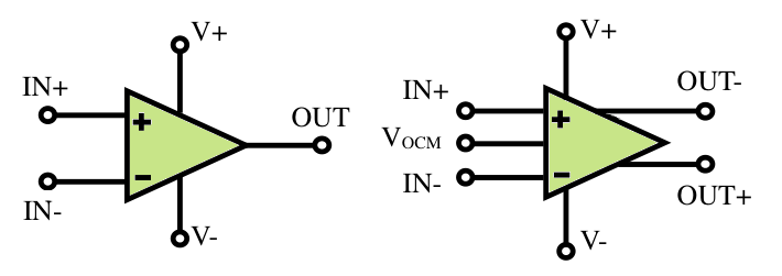
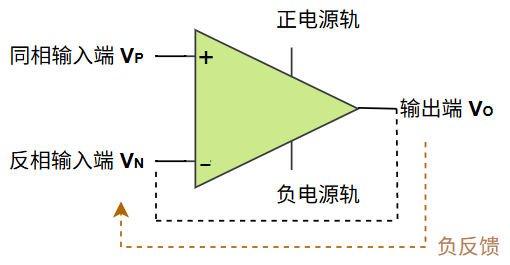
Figure 1: Standard op-amp circuit symbol. The
+terminal is the non-inverting input (output is in phase with it), and the−terminal is the inverting input (output is out of phase). Two inputs, one output, plus dual power supply rails—these are all the “interfaces” an op-amp needs.
2. The Op-Amp Family Tree: More Than Just One Type
Many beginners think “an op-amp is just an op-amp,” but in reality, after decades of development, op-amps have diversified into numerous specialized types. Understanding this family tree helps you make informed choices during component selection.
| Type | Key Characteristics | Typical Applications |
|---|---|---|
| General-Purpose Op-Amps (e.g., LM358, μA741) | Balanced performance, low cost | Education, low-frequency signal processing |
| Precision Op-Amps (e.g., OP07, OPA277) | Input offset voltage V_{OS} < 1\text{mV}, extremely low drift | Precision measurement, instrument front-ends |
| Rail-to-Rail Op-Amps (RRIO) | Input/output can swing very close to power rails | Battery-powered devices with low supply voltage |
| High-Speed Op-Amps | Very high slew rate (SR), wide bandwidth | High-speed ADC driving, video signals |
| Low-Noise Op-Amps (e.g., NE5532) | Extremely low noise density | Audio preamplifiers, Hi-Fi equipment |
| Instrumentation Amplifiers (e.g., AD620) | Extremely high CMRR, very high input impedance | Bridge sensors, ECG |
| Current Sense Amplifiers | Operate under common-mode voltages far above their own supply voltage | Battery charge/discharge monitoring, motor current sensing |
| Transimpedance Amplifiers (TIA) | Convert current input to voltage output | Photodiode amplification |
| Differential Op-Amps | Amplify difference between inputs, reject common-mode signals | Differential signal transmission |
| Isolation Amplifiers | Capacitive/magnetic/optical isolation between input and output | Medical devices, high-voltage safety |
| Programmable Gain Amplifiers (PGA) | Gain adjustable via digital signal | Auto-ranging systems |
Beginner Tip: Don’t memorize blindly. For any project, ask three questions: Is the signal frequency high? Is precision critical? Is power voltage low? These three questions usually narrow it down to the right type.
3. Open-Loop Use: When an Op-Amp Becomes a Comparator
3.1 Open-Loop Gain: The Op-Amp’s “Innate Superpower”
An op-amp comes with a natural superpower: open-loop gain (A_{OL}). What does “open-loop” mean? It means there’s no connection—no feedback network—between the output and input terminals.
In this state, the op-amp’s behavior is described by a simple formula:
Where:
- V_P: Voltage at non-inverting input
- V_N: Voltage at inverting input
- A_{OL}: Open-loop gain (typically 100,000× or more, i.e., 100 dB)
- V_O: Output voltage
What does this mean? Even a mere 1 mV difference between inputs, when amplified 100,000×, should theoretically yield 100 V output. But reality hits: you can’t output 100 V—your power supply limits the maximum output voltage.
3.2 Power Rails: The Op-Amp’s “Ceiling” and “Floor”
Op-amps require power. There are two common power configurations:
- Dual Supply: e.g., \pm 12\text{V}, allowing output to swing both above and below ground (0 V), enabling both positive and negative outputs.
- Single Supply: e.g., +12\text{V} and GND, restricting output between 0 V and +12\text{V}.
These supply voltage limits are called power rails. The output voltage can never exceed these rails—just as you can’t jump high enough to break through the ceiling.
Analogy: Open-loop gain is like someone capable of lifting 1,000× their body weight, but constrained by floor and ceiling. No matter their strength, their hand’s highest and lowest reach is limited. The “ceiling” is the positive rail; the “floor,” the negative rail (or ground).
3.3 Comparator Mode: Either 0 or 1
Combine the open-loop gain with rail-limited output, and you get the op-amp’s simplest operating mode—the comparator:
| Condition | Output |
|---|---|
| V_P > V_N (non-inverting input higher) | V_O ≈ positive rail |
| V_P < V_N (inverting input higher) | V_O ≈ negative rail |
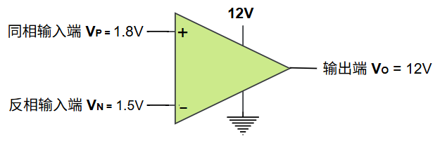
Figure 2: When V_P = 1.8\text{V}, V_N = 1.5\text{V}, V_P - V_N = +0.3\text{V} > 0, the op-amp output is “pushed” to the positive supply rail (here, +12\text{V}).
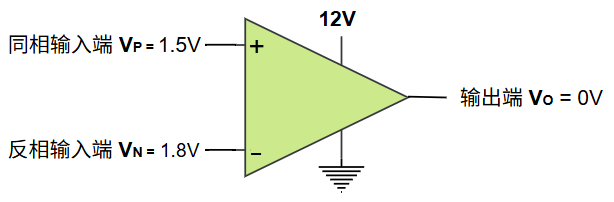
Figure 3: When V_P = 1.5\text{V}, V_N = 1.8\text{V}, V_P - V_N = -0.3\text{V} < 0, output is “pulled” to negative rail (here, 0\text{V}, single supply).
In short, an open-loop op-amp acts like a binary referee—it only judges which input is larger and gives an extreme result. This behavior resembles a dedicated comparator chip.
Practical Tip: While you can use a general-purpose op-amp as a comparator, it’s not recommended for high-speed or precise comparison. Reasons:
(1) Op-amps take time to recover from saturation—much slower than dedicated comparators;
(2) Most op-amps lack built-in hysteresis, so input noise can cause output jitter;
(3) Some op-amps may exhibit “phase reversal” under deep saturation. For reliable signal comparison, use a dedicated comparator (e.g., LM393).
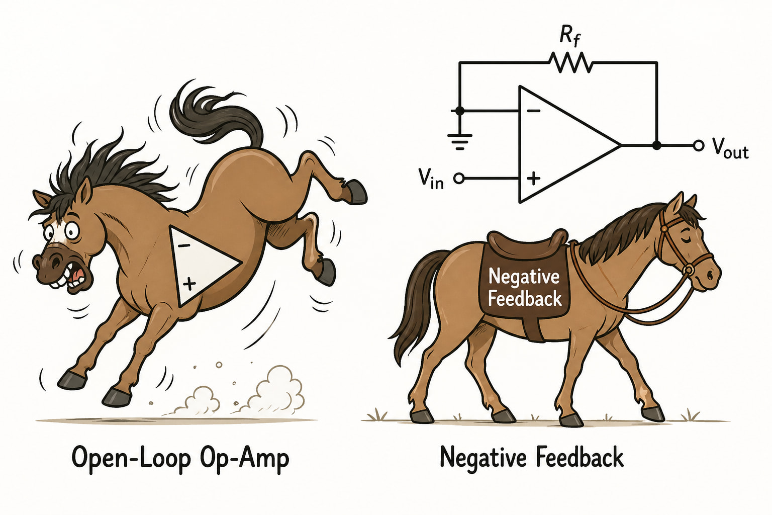
4. Introducing Negative Feedback: From Wild Horse to Tamed Steed
An open-loop op-amp is too “wild”—its enormous gain makes linear amplification impossible; any tiny input fluctuation sends the output slamming into the rails. To tame this “wild horse,” we use a technique: negative feedback.
4.1 What Is Negative Feedback?
Imagine adjusting shower temperature. You test the water (sense output), turn down hot if it’s too hot, turn up if too cold. You continuously sense, compare, and adjust until the water stabilizes. This is negative feedback—feeding a portion of the output back to the input to oppose deviations.
In op-amp circuits, negative feedback means connecting the output V_O back to the inverting input V_N via resistors or other components. Then:
- If V_O is slightly higher than desired → feedback voltage to V_N increases → V_P - V_N decreases → op-amp reduces output
- If V_O is slightly lower → feedback voltage to V_N decreases → V_P - V_N increases → op-amp boosts output
This closed-loop self-adjustment happens extremely fast (typically microseconds), ultimately stabilizing the output at a precise value.
Analogy: An open-loop op-amp is like a car with the gas pedal floored—either full speed or stopped. With negative feedback, it’s like adding cruise control—you set a desired speed (V_P), and the system automatically adjusts the throttle (V_O) to match.
5. Voltage Follower: The Most Basic and Practical Circuit
5.1 Circuit Configuration
Connect the op-amp output V_O directly with a wire back to the inverting input V_N, and you get a voltage follower:
This might seem confusing: output directly tied to input? What’s the point? Isn’t output just equal to input?
Exactly! That’s its purpose. The output voltage equals the input voltage (gain = 1), but it boasts extremely high input impedance and extremely low output impedance. In plain terms: it draws almost no current from the source, yet can deliver substantial current to the next stage.
5.2 Real-World Analogy
Imagine copying a famous painting. You can’t press hard on the original (high input impedance), but you want a perfect copy (output = input) and you can press firmly on the copy paper (strong drive capability).
The voltage follower acts as a buffer—it creates an “isolation wall” between source and load. The source feels nothing is connected (high input Z), while the load sees a powerful driver (low output Z).
5.3 When to Use a Voltage Follower?
- High-impedance sensors (e.g., thermistor or photodiode voltage divider nodes) can’t directly drive ADCs—add a voltage follower.
- Multiple circuits need to share a reference voltage without mutual interference—put a follower in each branch.
- For long signal lines, use a follower at the receiving end for impedance matching.
6. Non-Inverting Amplifier: Signal Direction Preserved, How Much Gain?
6.1 Circuit Configuration
In a non-inverting amplifier, the input signal enters the non-inverting terminal. The feedback network (resistors R_1 and R_2) connects between the output and inverting input:
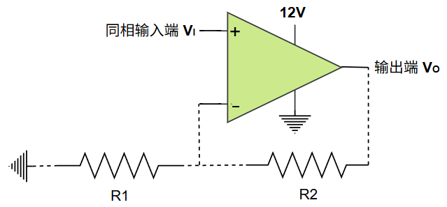
- R_1: From inverting input to ground (gain resistor R_G)
- R_2: From output to inverting input (feedback resistor R_F)
6.2 How Deep Negative Feedback Auto-Regulates
Let’s walk through the process. Assume V_I = 1\text{V}, R_1 = R_2 = 1\text{k}\Omega:
- V_P = V_I = 1\text{V} (signal applied directly)
- At power-on, V_O \approx 0\text{V}, so via R_2 and R_1 divider, V_N \approx 0\text{V}
- V_P - V_N = 1\text{V} - 0\text{V} = +1\text{V} > 0, so op-amp “pushes” output upward
- As V_O rises, V_N = V_O \cdot \frac{R_1}{R_1 + R_2} also rises
- When V_O = 2\text{V}, V_N = 2 \cdot \frac{1\text{k}}{1\text{k}+1\text{k}} = 1\text{V} = V_P
- Now V_P - V_N = 0, so output stabilizes at 2\text{V}
Result: 1 V input, 2 V output—gain of 2!
6.3 Mathematical Derivation (Walk Through)
Use two key op-amp features under deep negative feedback:
- Virtual Short: V_P = V_N ⇒ V_N = V_I
- Virtual Open: No current into op-amp inputs ⇒ current through R_1 = current through R_2
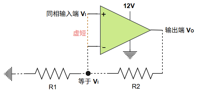
By Ohm’s law (I = U/R):
Current through R_1:
Current through R_2:
Set equal:
Solve:
$$V_OIf R_1 = R_2 = 1\text{k}\Omega, then A_V = -1, and the output waveform is a perfect mirror image (inverted) of the input.
7.5 Summary of Inverting Amplifier Characteristics
| Characteristic | Description |
|---|---|
| Gain formula | A_V = -R_2 / R_1 |
| Gain range | Can be < 1 (attenuation), or > 1 (amplification) |
| Input impedance | R_{in} \approx R_1 (low! This is the most important difference) |
| Output-to-input phase | Inverted (180° phase difference) |
7.6 Inverting vs. Non-Inverting: How to Choose?
| Comparison Dimension | Non-Inverting Amplifier | Inverting Amplifier |
|---|---|---|
| Input impedance | Extremely high (MΩ level) | Approximately equal to R_1 (typically kΩ level) |
| Gain range | \ge 1 | Any (can attenuate) |
| Phase | 0° | 180° |
| Common-mode voltage | Input terminals carry common-mode voltage | Input common-mode voltage ≈ 0V (virtual ground) |
| Typical use cases | High-impedance signal sources (e.g., sensors) | Low-impedance sources, or when inversion is needed |
- Does an inverting amplifier require dual power supply? Not necessarily. If the input signal is always positive (e.g. a 0–2V sine wave), you can use a single supply, but you must bias the non-inverting input to a mid-supply reference voltage (e.g. V_{CC}/2) instead of grounding it—this is known as “biasing.” If the input signal has both positive and negative components, a dual supply is required; otherwise, the negative portion of the output will be clipped.
- Input impedance issue: The input impedance of an inverting amplifier is equal to R_1. If you set R_1 = 1\text{k}\Omega, the signal source sees a 1\text{k}\Omega load. If the source has weak drive capability (high output impedance), the signal will be attenuated due to voltage division, leading to inaccurate measurements.
- The magic of virtual ground: Because the V_N node at the inverting input is always ~0V (virtual ground), this configuration is the foundation for summing amplifiers and current-to-voltage converters.
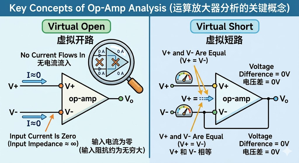
8. Virtual Short and Virtual Open: The “Twin Keys” to Op-Amp Analysis
Anyone learning op-amps will encounter two core concepts: virtual short and virtual open. These are the universal keys to analyzing all linear op-amp circuits. Many tutorials just say “memorize it,” but here we’ll explain their essence in everyday terms.
8.1 Virtual Open
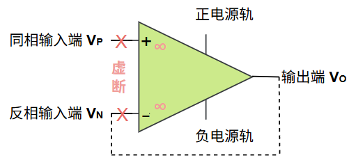
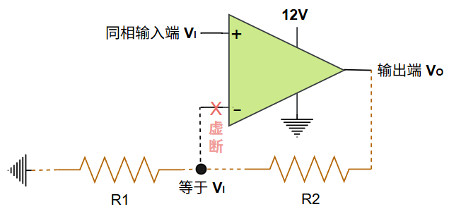
Definition: The input impedance of an op-amp is designed to be extremely high (ideally infinite), so almost no current flows into or out of the input terminals. It’s as though the inputs were disconnected—though not physically, hence “virtual” open.
Analogy: Imagine standing in front of a high-impedance electrostatic voltmeter. The probe can sense the static voltage on your body, but it draws almost no charge from you—you hardly feel its presence. The op-amp’s inputs act like such a “high-impedance voltage sensor.”
Key formula: I_P \approx 0, I_N \approx 0
8.2 Virtual Short
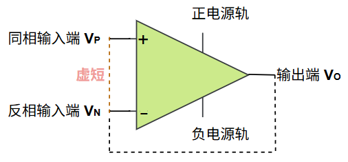
Definition: When an op-amp has deep negative feedback, the voltage at the non-inverting input (V_P) becomes almost equal to the voltage at the inverting input (V_N). It’s as though the two terminals are shorted together—but not actually, so we say “virtual” short.
Why does a virtual short occur?
This is a direct result of negative feedback. Recall the cruise control analogy from Chapter 4:
- The op-amp aggressively adjusts V_O until V_P - V_N \approx 0
- If V_P - V_N isn’t near zero, the op-amp continues to “push” or “pull” the output
- Only when V_P \approx V_N does the system reach equilibrium
So a virtual short isn’t an inherent circuit property—it’s enforced by negative feedback. Remove the feedback (open loop), and the virtual short vanishes: V_P and V_N can differ significantly.
Key formula: V_P \approx V_N (holds only under deep negative feedback)
8.3 Virtual Short + Virtual Open = Ultimate Analysis Tool
Used together, these two concepts turn analysis of nearly any linear op-amp circuit into middle-school math:
- Virtual short tells you V_P = V_N, giving you a known voltage at a critical node.
- Virtual open tells you no current flows into the inputs, so current through external resistors can be analyzed using Kirchhoff’s laws.
- The rest is applying Ohm’s Law and solving equations.
8.4 Common Pitfalls for Beginners
- Assuming virtual short always holds: Virtual short only applies under deep negative feedback and in the linear region. When the op-amp saturates (output hits the supply rails), virtual short fails.
- Thinking virtual open means nothing can be connected: Virtual open only means negligible current; voltage signals can still be applied. Inputs are, of course, meant to be connected to circuits.
9. Common Beginner Mistakes (Pitfall Avoidance Guide)
Mistake 1: Ignoring supply rails, treating gain formula as universal
“I set the gain to 100×, input 0.5V—why isn’t the output 50V?”
Because your supply voltage is only 5V! The gain formula describes ideal linear behavior, but output is always clamped by the supply voltage. The gain formula is the “dream”; supply rails are the “reality.”
Mistake 2: Using op-amps as comparators casually
General-purpose op-amps can act as basic comparators, but they’re slow, lack hysteresis, and may suffer phase reversal. For precision comparison, use dedicated comparators.
Mistake 3: Using single supply with inverting amplifier without biasing
In an inverting amplifier, the non-inverting input is grounded (0V), so output swings around 0V. With only a single supply (e.g., 0–5V), negative half-cycles get clipped. Fix it by biasing the non-inverting input to a reference like V_{CC}/2.
Mistake 4: Using extreme resistor values
- Resistors too small (e.g. 10\Omega) → excessive current, exceeds op-amp output drive, causes heating
- Resistors too large (e.g. 10\text{M}\Omega) → high thermal noise, significant errors from input bias current
Recommended range: 1\text{k}\Omega \sim 100\text{k}\Omega.
Mistake 5: Ignoring bandwidth limitations
Gain-bandwidth product (GBW) is constant. A gain of 100× limits bandwidth to GBW/100. To amplify a 100kHz signal with 100× gain, you need an op-amp with GBW ≥ 10MHz.
Mistake 6: Forgetting bypass capacitors
Always place a 0.1\mu\text{F} ceramic capacitor (bypass capacitor) near the op-amp’s power pins. Without it, the op-amp may oscillate—producing high-frequency noise at the output despite no input.
Mistake 7: Inputs exceeding common-mode range
Many op-amps have a common-mode input range smaller than their supply rails (non-rail-to-rail). If input voltage exceeds this range, the op-amp may behave abnormally or even invert phase.
10. Op-Amp Selection Guide: Matching Devices to Applications
10.1 Selection Decision Tree
Start Selection
│
├─ Signal frequency > 1MHz?
│   ├─ Yes → High-speed op-amp (SR > 50V/µs, GBW > 50MHz)
│   └─ No → Continue
│
├─ High precision required? (error < 0.1%?)
│   ├─ Yes → Precision op-amp (V_OS < 100µV, drift < 1µV/°C)
│   └─ No → Continue
│
├─ Low supply voltage? (< 5V?)
│   ├─ Yes → Rail-to-rail op-amp (RRIO)
│   └─ No → Continue
│
├─ High source impedance? (> 100kΩ?)
│   ├─ Yes → FET/CMOS input op-amp (I_B < 10pA)
│   └─ No → Continue
│
├─ Low noise critical? (audio / precision measurement?)
│   ├─ Yes → Low-noise op-amp (noise density < 10nV/√Hz)
│   └─ No → Continue
│
├─ Need current sensing?
│   ├─ Yes → Current-sense amplifier
│   └─ No → Continue
│
└─ No special requirements → General-purpose op-amp (LM358/LM324/TL074)
10.2 Application Quick Reference Table
| Application | Recommended Op-Amp Type | Key Parameters to Consider | Example Models |
|---|---|---|---|
| Battery-powered portable devices | Low power + Rail-to-rail | Quiescent current < 1mA, RRIO | MCP6002, TLV9002 |
| Audio preamplifier | Low noise + Low distortion | Noise density < 5nV/√Hz, THD+N < 0.001% | NE5532, OPA1612 |
| Temperature/pressure sensors | Precision + Low drift | V_{OS} < 100\mu\text{V}, drift < 1µV/°C | OP07, OPA277 |
| High-speed ADC driver | High speed + Wide bandwidth | SR > 50V/µs, settling time < 100ns | AD8051, THS4031 |
| Motor current sensing | Current-sense amplifier | Common-mode range > 30V, CMRR > 100dB | INA181, MAX4080 |
| Photodiode amplifier | Transimpedance amplifier (TIA) | Ultra-low I_B (< 1pA), low noise | OPA656, ADA4530-1 |
| ECG/EEG measurement | Instrumentation amplifier | CMRR > 100dB, ultra-low noise | AD620, INA128 |
| General teaching / low-frequency experiments | General-purpose op-amp | Inexpensive, readily available, robust | LM358 (dual), TL074 (quad) |
11. Key Parameter Deep Dive
11.1 DC Parameters (Static Characteristics)
These affect op-amp precision in DC and low-frequency applications.
| Parameter | English Name | Function and Layman Explanation | Desired Trend | Typical (General) | Typical (Precision) |
|---|---|---|---|---|---|
| Input offset voltage V_{OS} | Offset Voltage | “Built-in error” due to internal transistor mismatch. Even with equal inputs, the op-amp acts as if there’s a V_{OS} difference. | ↓ Smaller is better | 1–10 mV | < 100 µV |
| Offset voltage drift \frac{dV_{OS}}{dT} | Offset Voltage Drift | How much V_{OS} changes per 1°C temperature change. Often a bigger headache than initial V_{OS} in precision circuits, since drift is harder to compensate. | ↓ Smaller is better | 5–20 µV/°C | < 1 µV/°C |
| Input bias current I_B | Input Bias Current | Small “keep-alive” current required at inputs from internal transistor bases/gates. | ↓ Smaller is better | Bipolar: 10–200 nA; CMOS: < 1 pA | CMOS: < 10 pA |
| Input offset current I_{OS} | Input Offset Current | Difference between I_B at the two inputs. I_B can be cancelled with balanced resistors, but I_{OS} errors are harder to eliminate. | ↓ Smaller is better | 5–20% of I_B | 5–20% of I_B |
| Input voltage range | Input Voltage Range | Maximum input voltage range the op-amp can handle. Rail-to-rail (RRI) op-amps cover almost the full supply range. Non-rail-to-rail ones are limited (typically 1–2V below rails). | ↑ Larger is better | V_{SS}+1.5\text{V} \sim V_{DD}-1.5\text{V} (non-rail-to-rail) | V_{SS} \sim V_{DD} (rail-to-rail) |
| Output voltage swing | Output Voltage Swing | Actual maximum output voltage range. Similar to input, includes rail-to-rail output (RRO) vs. non-rail-to-rail variants. | ↑ Larger is better | V_{SS}+0.5\text{V} \sim V_{DD}-0.5\text{V} | Rail-to-rail: V_{SS}+10\text{mV} \sim V_{DD}-10\text{mV} |
11.2 AC Parameters (Dynamic Characteristics)
These describe op-amp behavior with AC signals.
| Parameter | English Name | Function and Layman Explanation | Desired Trend | Typical Values |
|---|---|---|---|---|
| Open-loop gain A_{OL} | Open Loop Gain | Amplification without feedback. Higher A_{OL} means feedback circuits achieve gain closer to theory. | ↑ Larger is better | 100–140 dB |
| CMRR | Common Mode Rejection Ratio | Ability to reject common-mode signals (same noise on both inputs). Formula: \text{CMRR} = 20\log\frac{A_d}{A_c}. High CMRR = amplifies only the difference, not the common part. | ↑ Larger is better | 70–120 dB |
| PSRR | Power Supply Rejection Ratio | Ability to block power supply ripple from affecting output. Crucial if power supply is noisy (e.g. switching supplies). | ↑ Larger is better | 70–100 dB |
| Slew rate SR | Slew Rate | Maximum speed of output voltage change (V/µs). Insufficient SR causes distortion on fast signals. Main cause of large-signal distortion. | ↑ Larger is better | General: 0.5–10 V/µs; High speed: > 50 V/µs |
| Settling time t_S | Settling Time | Time for output to stabilize within a specified precision after a step input. Critical for ADC drivers. | ↓ Smaller is better | General: 1–10 µs; High speed: < 100 ns |
| Phase margin \varphi_m | Phase Margin | At 0dB gain, how far the phase shift is from -180°. \varphi_m < 30° may cause oscillation. | ↑ Larger is better | 45°–60° (safe) |
| Gain margin GM | Gain Margin | At -180° phase shift, how many dB below 0dB the gain is. GM < 0dB → oscillation. | ↑ Larger is better | 10–20 dB (safe) |
| THD+N | THD + Noise | “Purity” of output signal. Lower values = cleaner signal. | ↓ Smaller is better | 0.01%–0.1% (general); < 0.001% (Hi-Fi) |
| Thermal resistance R_{\theta JA} | Thermal Resistance | Resistance from chip junction to ambient. Lower = better heat dissipation, higher power handling. | ↓ Smaller is better | Package dependent; SOT-23 ≈ 200°C/W, SO-8 ≈ 120°C/W |
11.3 Bandwidth Parameters
| Parameter | English Name | Function and Layman Explanation | Desired Trend | Typical Values |
|---|---|---|---|---|
| Unity gain bandwidth UGBW | Unity Gain Bandwidth | Frequency where open-loop gain drops to 1 (0dB). Above this, op-amp stops amplifying and begins attenuating. | ↑ Larger is better | ### 12.4 Experiment 3 (Optional Challenge): Inverting Amplifier |
- Connect the non-inverting input (pin 3) to ground.
- Apply the input signal to the inverting input (pin 2) through R_1 = 10\text{k}\Omega.
- Connect R_2 = 10\text{k}\Omega between the output (pin 1) and the inverting input (pin 2).
Note: The inverting amplifier produces a negative output (relative to ground). If you power the op-amp with a single 9V supply, it cannot output true negative voltages—so when measuring with a multimeter, the output might appear close to 0V (as the output tries to go below 0V but is limited by the negative supply rail). To “lift” the operating point, you can connect the non-inverting input to a reference voltage of V_{CC}/2 (about 4.5V) to verify the inverting amplification relationship.
12.5 Safety Tips for Experiments
- The LM358 is a single-supply op-amp. Never apply a negative voltage exceeding -0.3V, or the chip may be damaged.
- Always power off before soldering or plugging/unplugging components—working with power on is the leading cause of damaged chips among beginners.
- If the circuit “doesn’t work,” first use a multimeter to measure the voltage at each pin and compare it with your expectations. 90% of issues are due to wiring errors or forgotten power connections.
Appendix: Quick Reference Table of Classic Op-Amp Models
| Model | Type | Channels | Supply Range | GBW | SR | Features | Approx. Price |
|---|---|---|---|---|---|---|---|
| LM358 | General Purpose | Dual | 3V–32V (single) | 1 MHz | 0.6 V/µs | Inexpensive, rugged, single-supply friendly | ¥0.5 |
| LM324 | General Purpose | Quad | 3V–32V (single) | 1 MHz | 0.5 V/µs | Quad version, high cost-performance | ¥0.8 |
| TL074 | JFET Input | Quad | ±18V | 3 MHz | 13 V/µs | Low noise, high input impedance | ¥1.5 |
| NE5532 | Low-Noise Bipolar | Dual | ±3V–±20V | 10 MHz | 9 V/µs | Audio “holy grail,” extremely low noise | ¥2.0 |
| MCP6002 | Low-Power RRIO | Dual | 1.8V–6V | 1 MHz | 0.6 V/µs | Ideal for battery-powered applications | ¥0.8 |
| OP07 | Precision | Single | ±3V–±18V | 0.6 MHz | 0.3 V/µs | Classic precision op-amp, extremely low V_{OS} | ¥1.5 |
| OPA277 | Precision | Single | ±2V–±18V | 1 MHz | 0.8 V/µs | Ultra-low offset, low drift | ¥8.0 |
| AD8051 | High-Speed | Single | 3V–12V | 110 MHz | 145 V/µs | High-speed voltage feedback | ¥5.0 |
Quick Selection Guide:
- “Cheap and versatile” → LM358 / LM324
- “Precision measurement, budget no object” → OP07 / OPA277
- “Wide voltage range, high input impedance” → TL074 (JFET input)
- “For great audio quality” → NE5532
- “Battery-powered, low voltage” → MCP6002
- “Fast as lightning, for high-speed applications” → AD8051
Closing Thoughts: Operational amplifiers are among the core components in analog electronics. By mastering virtual short and virtual open, negative feedback, and fundamental topologies (voltage follower, non-inverting/inverting amplifiers), you’ll be able to analyze and design most beginner-level circuits. But theory alone isn’t enough—go buy a breadboard, a few LM358 chips, and some resistors, and run through the experiments above. The sense of achievement when you see the numbers on your multimeter match theoretical predictions—the realization that circuits truly do follow the rules—is something no textbook can offer.
Happy soldering, and best wishes on your learning journey!
This article contains approximately 7,800 words and is aimed at electronics beginners, reorganizing op-amp fundamentals using intuitive analogies and a hands-on perspective. For deeper topics (such as filter design, oscillators, PCB layout guidelines), refer to application notes from op-amp manufacturers (e.g., TI’s “Op Amps for Everyone”).