A few days ago, I helped a friend look at the order screenshot for his first four-layer board. He asked me which surface finish to choose: OSP was free, while ENIG cost ten-plus yuan more. Does paying more always mean getting something better?
I was confused by the same question back in the day. PCB shops package surface finishes as paid options, which makes it look like choosing between a clear or matte phone screen protector. But what it really determines is whether the board is easy to solder, how long it can be stored, and whether BGA packages will pass.
Taking this as an excuse, let’s sort through the common processes so you won’t have to flip a coin next time you place an order.
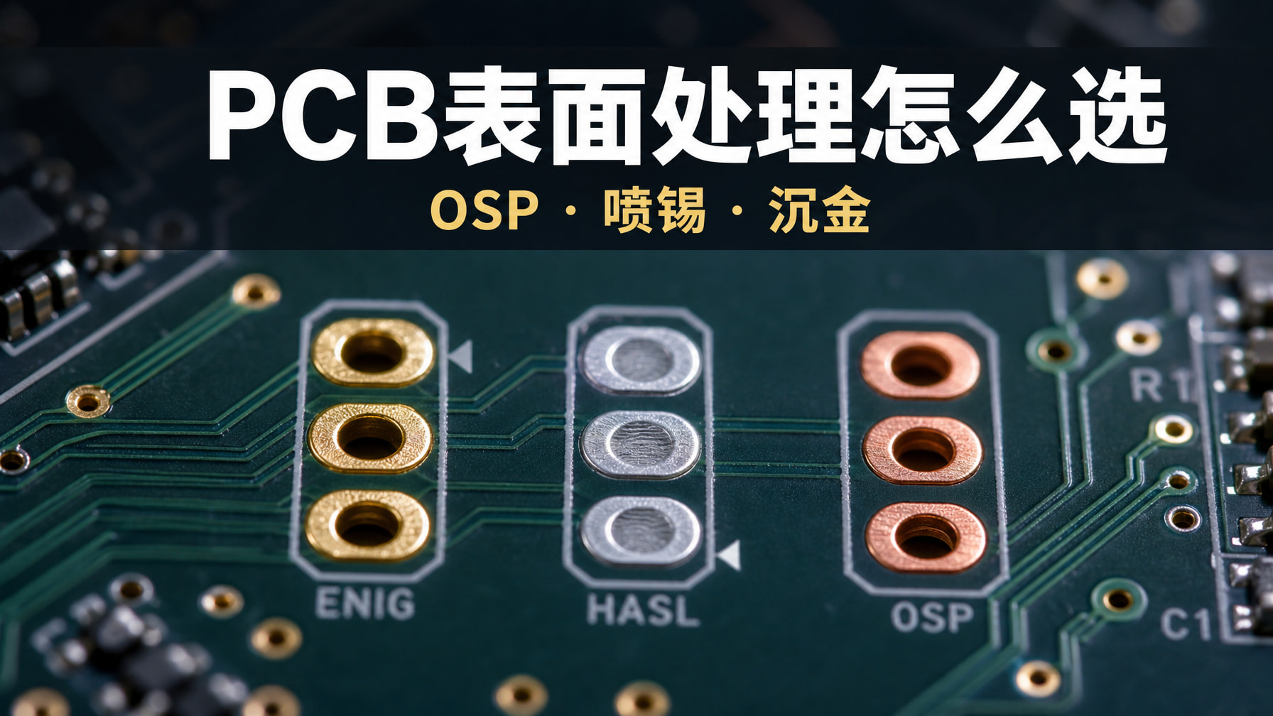
1. First, understand what this layer is protecting against
The pads on a PCB are made of copper. Copper is very reactive; after just a few hours exposed to air, it starts to discolor. After a month or two, the surface develops a layer of copper oxide and basic copper carbonate, turning black or green, and no matter how hard you press the soldering iron against it, the solder won’t wet.
That’s why the pad areas that the solder mask cannot cover must be coated with something before the board leaves the factory. This layer keeps the copper away from the air, then gets out of the way during soldering. Some processes plate a metal, while others apply an organic film, and these different approaches give us the options below.
2. OSP: it looks like nothing was done
OSP stands for Organic Solderability Preservative. The principle is that azole-based organic compounds complex with the copper surface, forming a transparent film about 0.2–0.5 micrometers thick.
When you receive the board, the pads are just the color of copper. The first time I used OSP, I thought the factory had skipped a step and inspected it under the light for ages.
You need to understand the shelf-life logic of this film. It is designed to escort the board through one reflow cycle. The flux and high temperature decompose the film, exposing fresh copper so soldering can take place. So OSP can only withstand one or two reflow cycles: the second is a stretch, and the third is basically naked copper. Double-sided SMT plus one rework brings it close to the limit.
Storage is just as precious. Unopened in a vacuum bag, it can last three to six months. Once opened, it’s best to place all the components within 24 to 48 hours. If you leave it on your bench collecting dust for two weeks and then try to solder it, even flux won’t save it.
The advantages are straightforward. It’s the cheapest; JLCPCB’s current free tier is all OSP. The film is only a fraction of a micrometer thick, so flatness is naturally excellent, with no issue for fine-pitch parts. The film is transparent, which means visual inspection can’t tell whether it’s good or bad. That can be seen as both a pro and a con; the downside is that you can’t tell whether it’s still alive.
Manual solderers have polarized feelings about OSP. My experience is that the first touch doesn’t tin very well and wetting is a bit slow, but adding more flux brings it back to normal. People used to HASL will find the switch uncomfortable.
3. HASL: the soldering-iron crowd’s white moonlight
HASL, or Hot Air Solder Leveling, is the technical name for spray tin. The board is dipped into a molten solder pot, then hot air blows off the excess solder, leaving a real layer of tin on the pads.
The leaded process uses Sn63/Pb37, with a melting point of 183°C. The lead-free version uses tin-silver-copper alloys such as SAC, with a melting point around 217°C, and the surface is more matte and rough.
HASL has top-tier solderability. The surface is already tin, the same family as the solder, so it wets as soon as the soldering iron touches it. Shelf life can reach about a year, it tolerates two or three reflow cycles, it’s rework-friendly, and you don’t feel bad if it gets scratched. In earlier years, it was absolutely the mainstream choice.
The disadvantages are also obvious. Wherever the hot air can’t level the surface evenly, solder peaks and pits remain. The surface has visible undulations and looks wavy under reflection. BGA and QFN packages with pitches below 0.5 mm can run into trouble on this surface: the solder volume on the two sides of the pad differs, and during reflow the component can be skewed. Thickness is also uneven, ranging from one or two micrometers in thin areas to tens of micrometers in thick areas. In addition, the whole board goes through a high-temperature solder pot, so the substrate undergoes thermal shock; large boards and thin boards are prone to warping.
There’s one more point: leaded HASL does not meet RoHS requirements, so don’t choose it if you need to export.
A counterintuitive fact: in the past couple of years, JLCPCB has basically removed HASL from free prototyping and standard orders, switching everything to OSP. The official reason is that complaints about poor tinning with HASL are far higher than with OSP. At first I didn’t understand that either: how could HASL have trouble wetting? Later I figured it out: on mass-production SMT lines, oxidation and solder dross on lead-free HASL surfaces cause more failures. Good for manual soldering and good for machines are two different things. What soldering-iron enthusiasts love and what an SMT production line prefers really don’t have to be the same surface finish.
4. ENIG: there’s a reason it costs more
ENIG stands for Electroless Nickel Immersion Gold, or electroless nickel/gold. It has a two-layer structure: first, a 3–6 micrometer chemical nickel layer is plated as the base, then a thin 0.05–0.1 micrometer gold layer is immersed on top.
Gold’s role here is like a bodyguard; nickel is the real body. Gold protects against oxygen during storage. When soldering actually happens, the gold dissolves into the solder, and the joint itself forms on the nickel underneath.
ENIG boards look golden, and their flatness is excellent, making them the standard choice for fine-pitch components. Shelf life can reach twelve months, they can handle three or more reflow cycles with ease, and double-sided SMT plus rework is no problem. JLCPCB’s paid prototyping option is ENIG; for a 10×10 board, spending ten-plus yuan more buys peace of mind.
There is one pitfall: black pad.
Immersion gold is a displacement reaction: gold ions bite nickel atoms out and replace them. If the chemistry is not controlled properly, the nickel surface becomes over-corroded, forming a phosphorus-rich black nickel layer. These pads look completely normal, shiny gold and all, but the truth comes out when soldered: the solder joints become brittle, fall off when bent, and the fracture surface is black. One criterion is phosphorus content at the fracture exceeding 15%. The probability is not that high, but when it happens, it’s batch-related: one bad batch can ruin a whole furnace load. There’s no rework fix; the entire batch has to be scrapped. For fields like military and medical where you can’t gamble, people pay extra for ENEPIG to eliminate the problem at the root, which I’ll discuss later.
There’s also a high-frequency cost to calculate. Nickel’s resistivity is more than four times that of copper, and it’s ferromagnetic. The skin depth is about 2 micrometers at 1 GHz and only 0.66 micrometers at 10 GHz, while the gold layer is less than 0.1 micrometers thick and cannot block it at all. Current on RF paths at the pads will flow substantially into the nickel layer, adding a few tenths of a dB of loss out of nowhere. That’s why millimeter-wave boards and RF test fixtures often avoid ENIG and use OSP or immersion silver instead. Spending the most money and botching the most critical part is something that often happens in RF.
5. Summary table
| Item | OSP | HASL | ENIG |
|---|---|---|---|
| Cost | Lowest | Low | High |
| Flatness | Good | Poor, solder peaks | Excellent |
| Solderability | Average, slow wetting | Best | Good |
| Shelf life | 3–6 months | 6–12 months | About 12 months |
| Reflow tolerance | 1–2 cycles | 2–3 cycles | More than 3 cycles |
| Fine-pitch BGA/QFN | Acceptable | Not suitable | Preferred |
| High-frequency loss | Low | Average | Higher at pads |
| Main risk | Invisible film failure | Unevenness, thermal shock | Black pad |
6. Less common on order pages, but you may still run into them
Immersion silver. A 0.1–0.4 micrometer layer of pure silver is immersed. Silver’s electrical conductivity is even higher than copper’s; measured line loss after immersion silver is only about 1–2% above the baseline, the best-looking result among the processes. Cost sits between OSP and ENIG. The pitfall is sulfur: sulfides in the air slowly make the silver surface turn yellow or black. Although this often doesn’t affect soldering, contact resistance can change, so long-term storage is a concern. It is widely used on high-speed digital and RF boards.
Immersion tin. About 1 micrometer of pure tin is immersed. It is flat, cheap, in the same family as the solder, and has excellent wetting. Press-fit connectors on backplanes specifically call for it. Two pitfalls: first, tin whiskers. Pure tin plating naturally tends to grow whiskers; over time they can bridge between fine-pitch pads and cause shorts, so high-reliability products avoid it. Second, tin and copper continuously interdiffuse to form intermetallic compounds, gradually consuming the pure tin layer itself, so shelf life is short too; it’s best used within six months. High-frequency loss is much worse than immersion silver, since tin’s resistivity is more than six times that of copper.
ENEPIG, electroless nickel/electroless palladium/immersion gold. A 0.1–0.2 micrometer palladium layer is inserted between the nickel and gold, separating the immersion gold solution from the nickel, which eliminates black pad at the mechanism level. The gold layer can also support gold wire bonding, making it the domain of COB processes, military, and medical applications. There is only one downside: it’s expensive, so you basically never see it on hobby boards.
Electroplated hard gold. This is an electroplated nickel/gold layer with cobalt added to the gold to increase hardness, with a thickness of 3 micrometers or more, specifically for wear from insertion and removal. The gold fingers on memory modules and graphics cards are made this way. Only the required areas are plated; the remaining pads still use ENIG or OSP. Plating the entire board with hard gold is a money-burning move. If your board has button contacts, gold fingers, or edge connectors, remember to mention it in the order notes.
7. So which one should I choose?
Copy the homework by scenario.
| Your situation | Recommended process |
|---|---|
| BGA or 0.4 mm-pitch QFN | ENIG |
| Board will be stored for more than six months before soldering | ENIG |
| Double-sided SMT plus rework, more than two reflow cycles | ENIG |
| Mass-produced consumer electronics, single SMT run, cost locked down | OSP |
| Prototype validation, no fine-pitch components | OSP, use the free tier |
| Mostly manual soldering, frequent rework | HASL, find a shop that still offers it |
| High-speed RF, PCIe, DDR5, millimeter wave | Immersion silver or OSP, avoid nickel |
| Gold fingers, buttons, insertion/removal areas | Hard gold plating, ENIG on the remaining pads |
| COB bonding, high reliability | ENEPIG |
| Backplane press-fit connectors | Immersion tin |
My default is this: for two-layer or four-layer prototypes with no BGA, use free OSP; if there’s a BGA or the board has to support production, use ENIG. The extra ten-plus yuan is far cheaper than reworking a BGA. For boards I solder by hand, I look for a small shop that still offers HASL.
From today on, you can choose that field on the order page with your eyes closed.
References · JLCPCB official announcement (free prototyping OSP replacing HASL) · LCSC ENIG and gold plating primer · Jiepei surface finish signal integrity comparison · NCAB detailed explanation of PCB surface finishes · 21ic ENIG black pad failure analysis