First, to answer your question: it’s not the auxiliary winding — your VCC waveform proves exactly that.
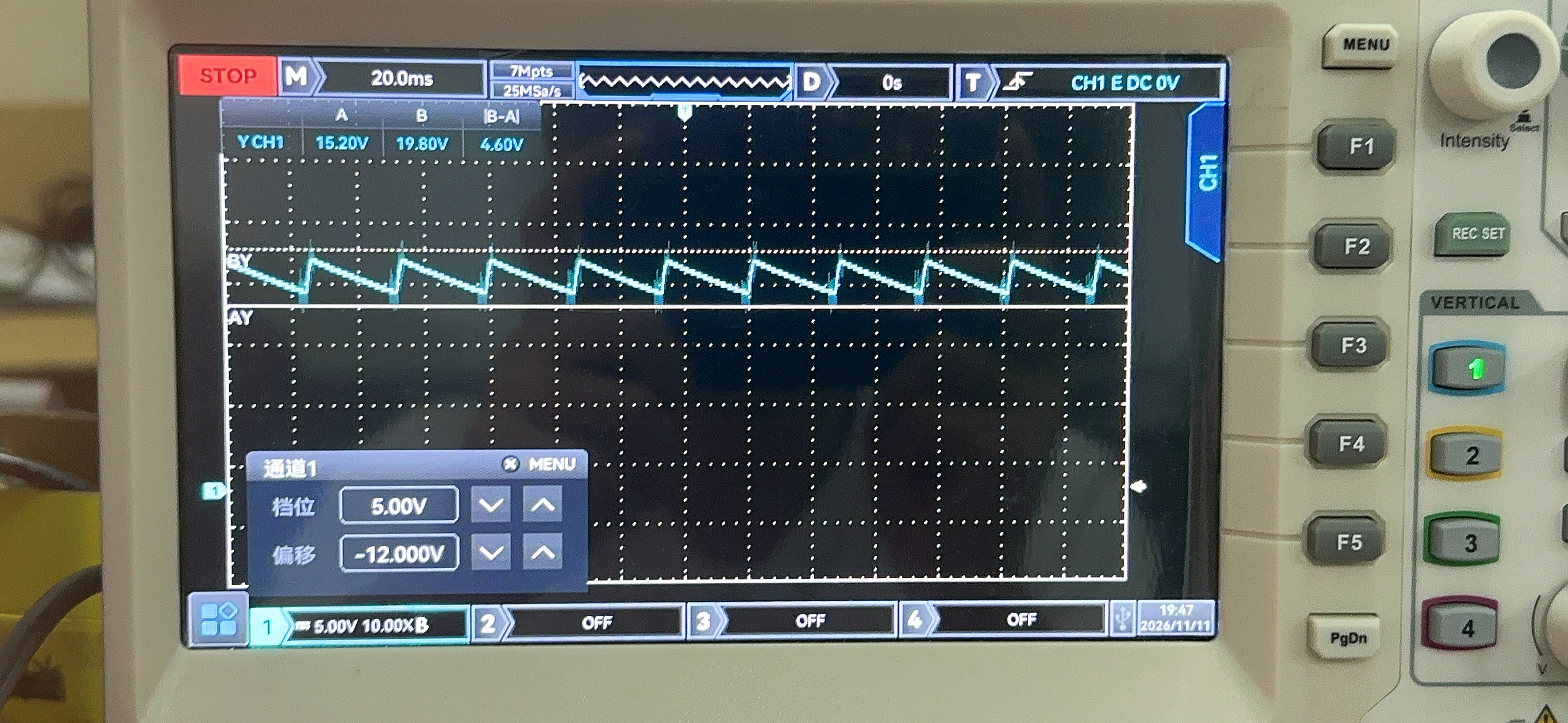
UC3842’s undervoltage lockout is 16 V turn-on, 10 V turn-off. Your Figure 2 shows VCC swinging between 15.2 V and 19.8 V — even the lowest point is above the startup threshold, more than 5 V away from the turn-off threshold. The chip is operating normally the whole time; there’s no power-down restart. When the auxiliary winding is genuinely starving and the converter hiccups, VCC draws a large sawtooth between 16 V and 10 V with a period of a few tenths of a second — completely different from what you have. So don’t touch the transformer.
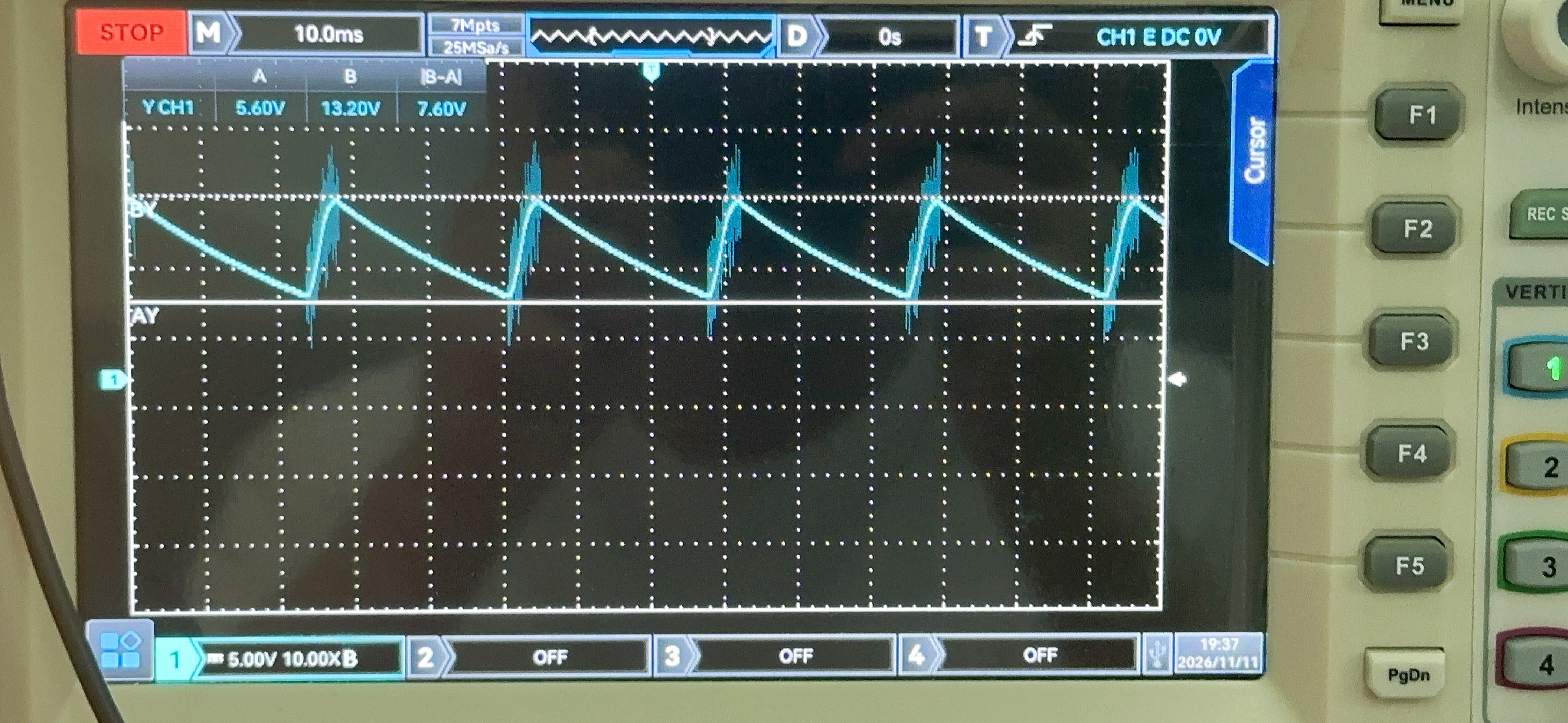
So what is this? Intermittent operation, also called pulse bunching. Break Figure 1 down:
-
The slow linear drop = the switch is basically idle and the output capacitor is discharging into the load;
-
The burst of high frequency on the rising edge = the switch suddenly runs for a short burst and charges the capacitor back up. The same-frequency VCC sawtooth matches this too: during the burst, the auxiliary winding supplies heavily and pushes VCC up to 19.8 V; during the pause, it slowly drains down to 15.2 V. The two waveforms are two sides of the same “run–pause” cycle.
But a 7.6 V swing is not right. With normal light-load pulse skipping, the output should fluctuate slightly around the setpoint, on the order of a few hundred millivolts. Yours goes from 5.6 V to 13.2 V, and the valley is far below the setpoint — this means the loop can hold the high end but can’t pull the low end back; the feedback response can’t keep up — this is not a “normal light-load phenomenon.”
First, run one experiment to narrow it down: attach a dummy load. For a 12 V output, use 100 Ω/5 W (about 120 mA) or 51 Ω/10 W (about 235 mA).
-
If it becomes stable with the load attached → light-load intermittent operation; add a minimum dummy load and then adjust compensation.
-
If it still swings with the load attached → check the loop; continue below.
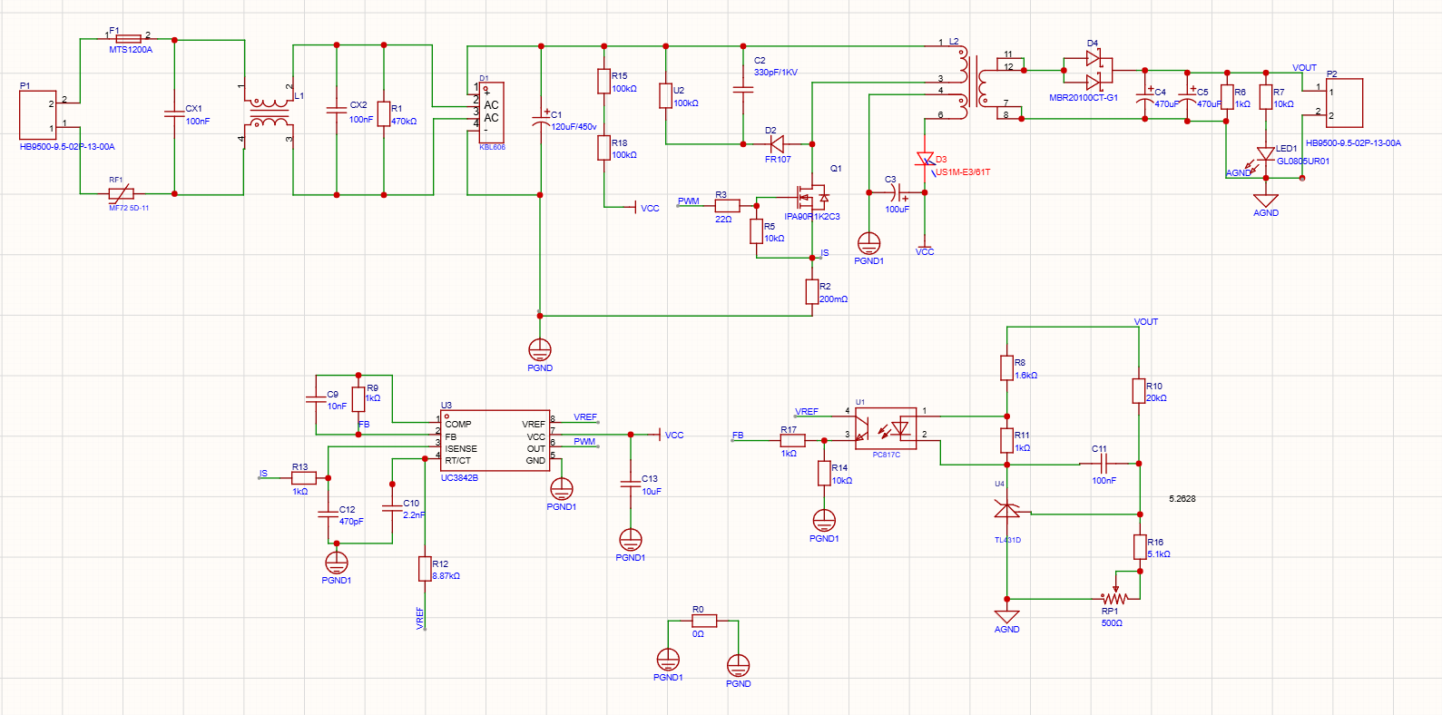
Check the loop in this order; each item maps directly to something on the schematic:
-
Measure how the DC level at COMP (pin 1) changes over one cycle: a slow ramp = the loop is too slow; it stays high but the output still drops = the power stage can’t supply enough (transformer saturation or current limiting).
-
Measure whether TL431 REF is 2.5 V, and also confirm that potentiometer RP1 has good contact.
-
Look at the compensation network: between COMP and FB you have 1 k + 10 nF in series, with a zero at 15.9 kHz. That’s on the fast side, and the low-frequency integral action is weak. A common approach is 4.7 k + 10 nF from COMP to ground, plus 10 k + 100 pF in series from COMP to VREF.
-
Watch the optocoupler LED current: when the output drops to 5.6 V, with R8 = 1.5 k only about 1.3 mA remains. TL431 may not reach its 1 mA minimum operating current, making the feedback even weaker — this amplifies the swing and creates a vicious cycle.
Finally, set the timebase to 20 µs/div and look at the burst section: check the Vds plateau, the gate-drive duty cycle, and especially whether ISENSE hits 1 V every cycle — if it does, it’s current limiting and the power stage can’t supply enough.
Don’t go down the subharmonic path; that’s the wide/narrow pulse alternation at fsw/2 (about 44 kHz), which has nothing to do with your 50 Hz.
Good news: you can stop suspecting the auxiliary winding, because your own scope shot just acquitted it.
The 3842 turns on at 16 V and off at 10 V. Your VCC is wandering between 15.2 and 19.8 V. It never even gets down to the turn-on threshold, let alone the dropout. The chip’s been awake the entire time. Real aux starvation is a completely different animal — VCC saws from 16 V down to 10 V over a few hundred milliseconds while the output repeatedly dies and restarts. Not what you’ve got. Put the transformer down.
What you have got is the converter working in bursts. That slow straight ramp down on the output is just the output caps discharging into the load while nothing much is switching, and that messy rising edge is a quick burst of switching topping them back up. VCC does the same dance — shoots up to 19.8 V while it’s switching, sags to 15.2 V while it’s idling. Nicely consistent, actually.
But here’s the bit that isn’t right: a 7.6 V swing. Light-load burst on a healthy supply wobbles the output by a few hundred millivolts around the setpoint. Yours drops to 5.6 V, which is nowhere near 12 V. So the loop is catching it on the way up and completely failing to catch it on the way down. The feedback is too slow, or it’s not really in the game at all.
Do this first, it’s a two-minute experiment: stick a dummy load on the output — 100 Ω, 5 W (about 120 mA), or 51 Ω, 10 W if you want a sterner test.
-
Goes quiet → it was light-load burst all along. Leave a bleed resistor on there, job done.
-
Still swinging → now we dig into the feedback.
And here’s one I’d genuinely check early, because it’s a sneaky one in your exact circuit. Your optocoupler LED resistor is R8 = 1.5 k. At 5.6 V output there’s only about 1.3 mA going through that LED — and a TL431 wants roughly 1 mA of its own just to stay alive. So the lower the output sags, the feebler the feedback gets, and the feebler the feedback, the further it sags. That’s a swing amplifier right there. Try R8 at 1 k and see what happens.
Also worth a look: your COMP–FB network is 1 k and 10 nF, which puts the zero up around 16 kHz — quite brisk, not much low-frequency integration. A combo I’ve had good luck with is 4.7 k + 10 nF from COMP to ground and 10 k + 100 pF from COMP to VREF, then give it a load step and watch how it settles.
And do yourself a favour — put the timebase on 20 µs/div during one of those bursts. Look at the gate drive, look at the Vds plateau, and especially watch whether ISENSE is smacking into 1 V every single cycle. If it is, you’re current-limited and the power stage can’t keep up, which is a different fix entirely.
One last thing: don’t add slope compensation for this. Sub-harmonic wobble shows up around half the switching frequency — 44 kHz on your timing values — as alternating fat and thin pulses. Yours is 50 Hz. Wrong postcode.
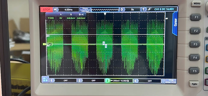
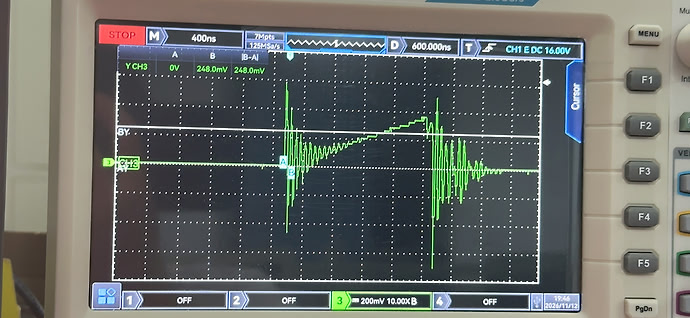
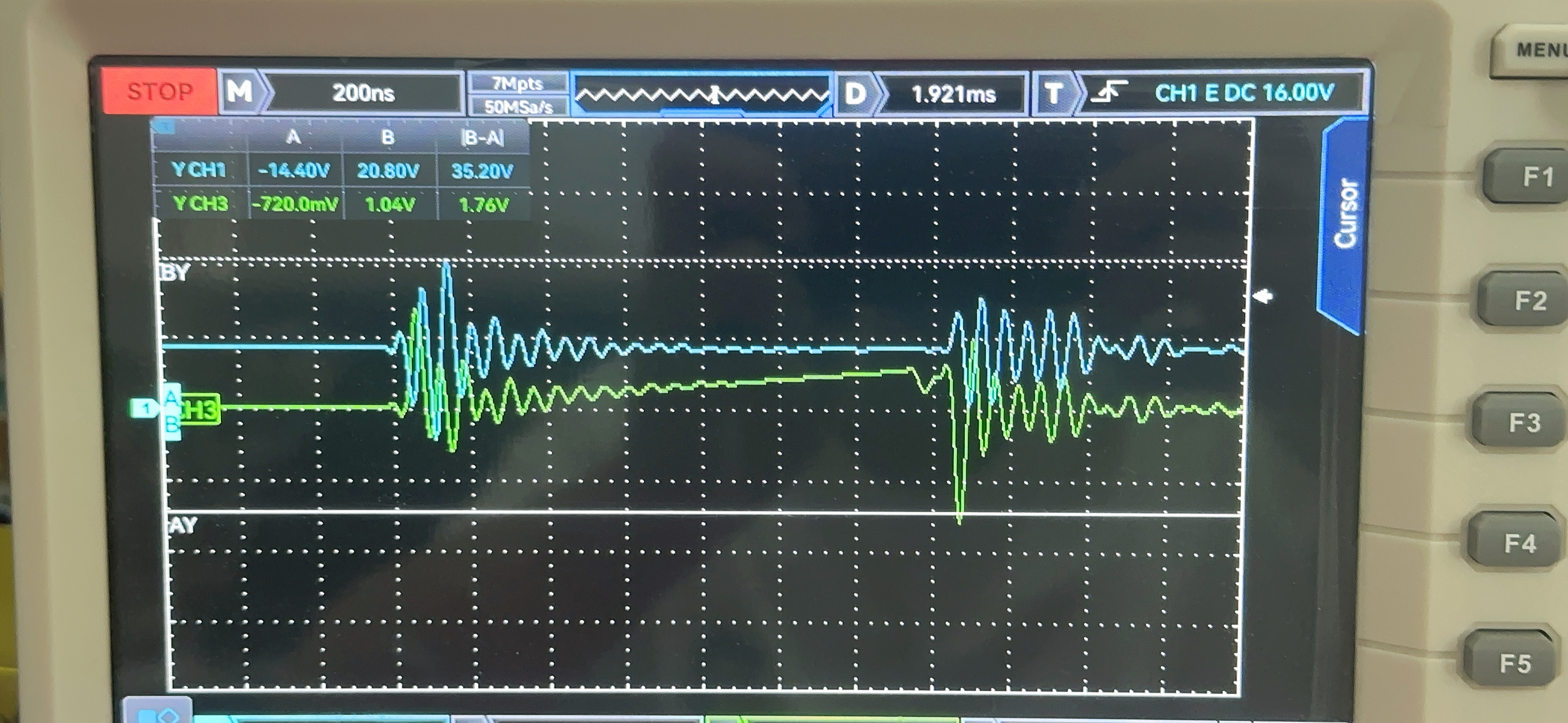
Thank you. I’ll now try out the method you mentioned, and here are some additional waveforms from my earlier tests — could you take a look and see if they make the problem easier to identify? The first and second images show waveforms from my 200 mΩ sampling resistor. The third shows the output and sampling resistor together (blue is the output waveform, green is the sampling resistor waveform).
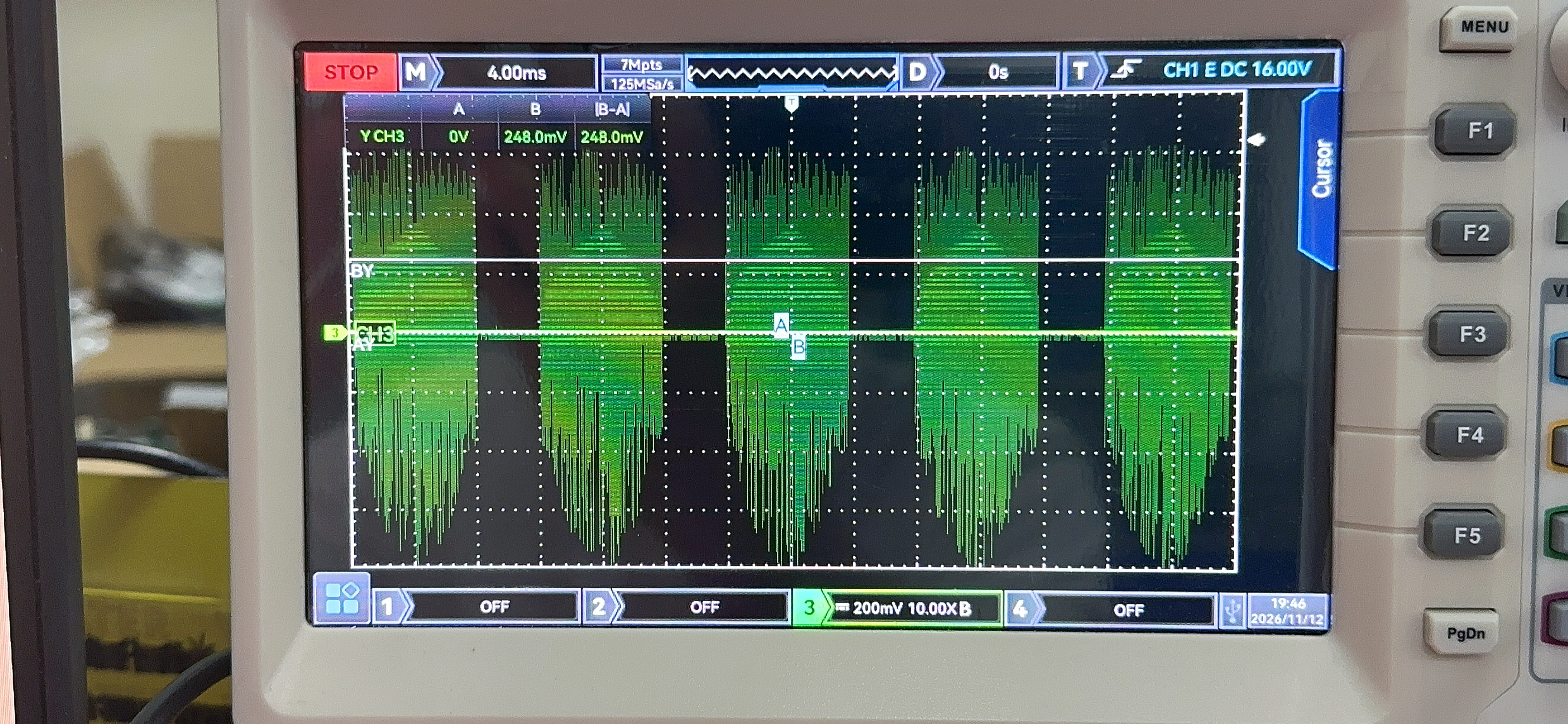
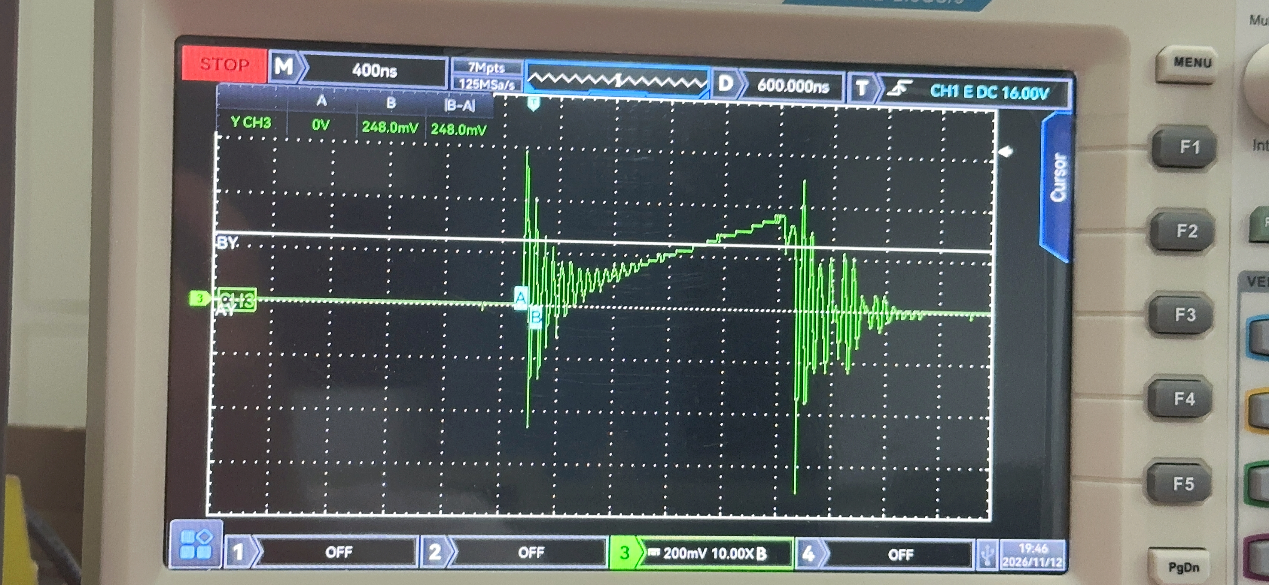
Thanks, I’ll debug the method you mentioned now, and then below are some supplementary waveforms from my earlier tests—please take a look and see whether the problem can be identified more clearly. The first and second images are the waveforms of my 200 mΩ sampling resistor. The third is the waveform of the output terminal together with the sampling resistor (blue is the output terminal waveform, green is the sampling resistor waveform).
[“image|690x223”]
My flyback is designed for a 100 kHz / 12 V / 5 A output. I changed the LED current-limiting resistor to 1K, and when I tested it with a 10-ohm load, the waveform was still basically the same. Below, the blue waveform is the output voltage, and the green waveform is the current-sense resistor at the low side of the MOSFET.
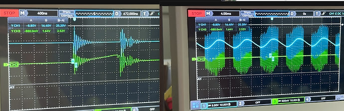
Once the new plot is out, anyone who was guessing current limiting can give it a rest. 248 mV divided by 200 mΩ is 1.24 A; the 3842’s 1 V threshold corresponds to 5 A, so it isn’t even a quarter of the way there. The ramp still rises smoothly and steadily, the transformer isn’t saturating, and the current loop isn’t intervening. The VCC trace is even less of a concern. With all three paths ruled out, only one place remains: COMP.
Go look at section 7.3.8 of TI’s UCx84x datasheet. It states clearly that the chip has two shutdown paths: one is ISENSE pulled above 1 V, and the other is COMP pulled below about two diode drops (1–1.4 V). The PWM latch is reset-dominant, so as long as the condition holds, the output stays low. The old Unitrode application note simply says “pull pin 1 below 1 V.”
Apply that to your 4 ms/div trace: between bursts there is a clean zero line—it’s not that the duty cycle gets smaller, it’s that the chip isn’t emitting a single pulse. So the whole process is: the output shoots up to 13.2 V, TL431 pulls the optocoupler hard, COMP gets forced into the shutdown region, and switching stops entirely; the output capacitor discharges through the load, falling all the way to 5.6 V; TL431 releases, COMP snaps back, and it fires a burst to pump the capacitor back up; then it overshoots again and shuts down again. COMP just bounces back and forth between “saturated high” and “shutdown low” and never spends any time in the linear region at all. This is a relaxation oscillation—it’s not the loop being “a bit slow”; the loop isn’t operating closed-loop at all.
So don’t rush to replace the compensation capacitor. First put a channel on pin1 and watch one complete 20 ms period; you’ll most likely see square-wave-like two-state transitions. That one measurement is far more direct than looking at the output waveform. At the same time, attach a 100 Ω/5 W dummy load. If it stabilizes as soon as you connect it, that means light load is pushing COMP into the shutdown region. Leave a minimum load, drop R8 from 1.5 k to 1 k so there is still more than 2 mA of LED current at the valley, then go back and adjust R9/C9.
By the way, one number: at 13.2 V output the LED current is about 6.3 mA; at 5.6 V it’s only 1.3 mA—a fivefold change within one cycle. The PC817C’s CTR is inherently nonlinear in this range, and the loop gain swings along with the output. The problem with this board isn’t in the power stage; it’s that the feedback has sent the gain flying.