Open-sourcing a wide-input-voltage, 24V3A output flyback switch-mode power supply (Flyback Power Supply), 72-watt power, up to 87.4% efficiency, based on the UC3842 chip with synchronous rectification (UCC24612-1DB), including detailed calculation processes for circuit and transformer parameters, schematic diagrams, PCB layout, PSIM simulation model, transformer manufacturing specification, and more.
Preface
![]() This is my first attempt at designing a flyback power supply. Please feel free to point out any areas that could be improved or corrected.
This is my first attempt at designing a flyback power supply. Please feel free to point out any areas that could be improved or corrected.
- Tutorial on Flyback Power Supply Parameter Calculations & Component Selection, Transformer Design & Winding: https://blog.zeruns.com/archives/909.html
- Guide to Magnetic Components / Core Materials / Core Structure Analysis, Comparison, and Selection: https://blog.zeruns.com/archives/897.html
![]() Also, I’m currently looking for job opportunities — any employers in Guangzhou, Foshan, or Shenzhen who are hiring, please consider me! You can check out my open-source projects on my LCSC Open Source Platform profile: https://oshwhub.com/zeruns/works
Also, I’m currently looking for job opportunities — any employers in Guangzhou, Foshan, or Shenzhen who are hiring, please consider me! You can check out my open-source projects on my LCSC Open Source Platform profile: https://oshwhub.com/zeruns/works
Project video demonstration: https://www.bilibili.com/video/BV1ES4GzQE19/
LCSC Open Source Platform link: https://oshwhub.com/zeruns/24v3a-Flyback-Power-Supply-uc384x
Electronics/MCU Technical Discussion QQ Group: 2169025065
Download links for all design files are at the end of this article!
![]() Warning: Building switch-mode power supplies involves significant risks. I do not guarantee the accuracy of any circuits, parameters, or formulas provided in this design. Replicating or referencing this project is done entirely at your own risk.
Warning: Building switch-mode power supplies involves significant risks. I do not guarantee the accuracy of any circuits, parameters, or formulas provided in this design. Replicating or referencing this project is done entirely at your own risk.
Estimated unit cost for small batch production (20 units): ~¥25 (excluding PCB and transformer, calculated using component prices from LCSC Mall). Including PCB and transformer, total cost should remain under ¥50.
Design Specifications
| Parameter | Value |
|---|---|
| Nominal Input Voltage V_{acnom} | 220VAC |
| Minimum Input Voltage V_{acmin} | 85VAC |
| Maximum Input Voltage V_{acmax} | 265VAC |
| Line Frequency f_L | 50Hz |
| Output Voltage V_{out} | 24V |
| Output Current I_{out} | 3A |
| Switching Frequency f_s | 150kHz |
| Target Efficiency η | 85% |
PCB Dimensions: 100 x 55 mm
PCB Specification: Double-layer board, through-hole components on top layer, SMD components on bottom layer
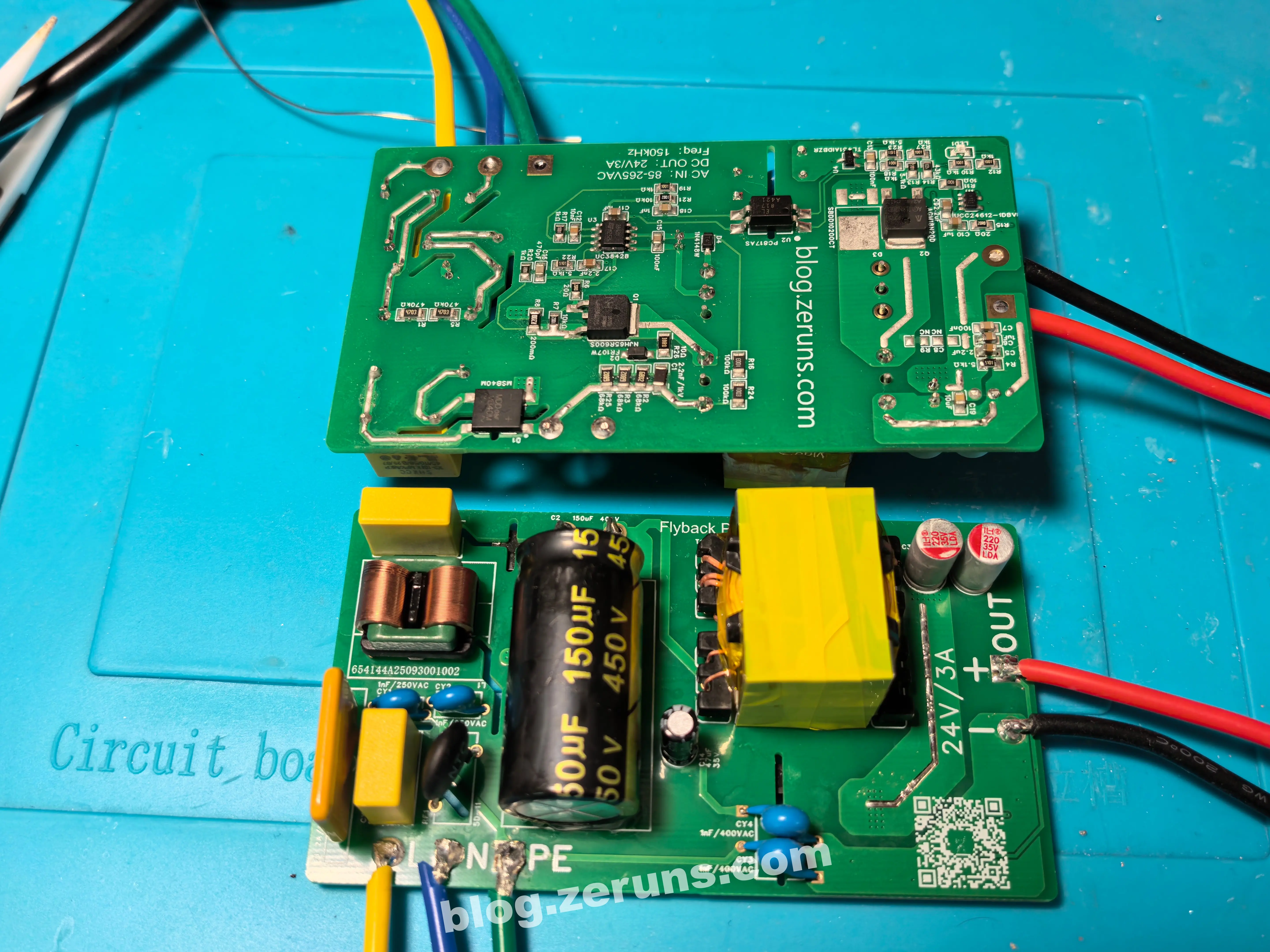
Physical Prototype Images
Below is the second revision:
Below is the first version — it had issues and was prone to MOSFET failure. The second version (above) has been fixed:
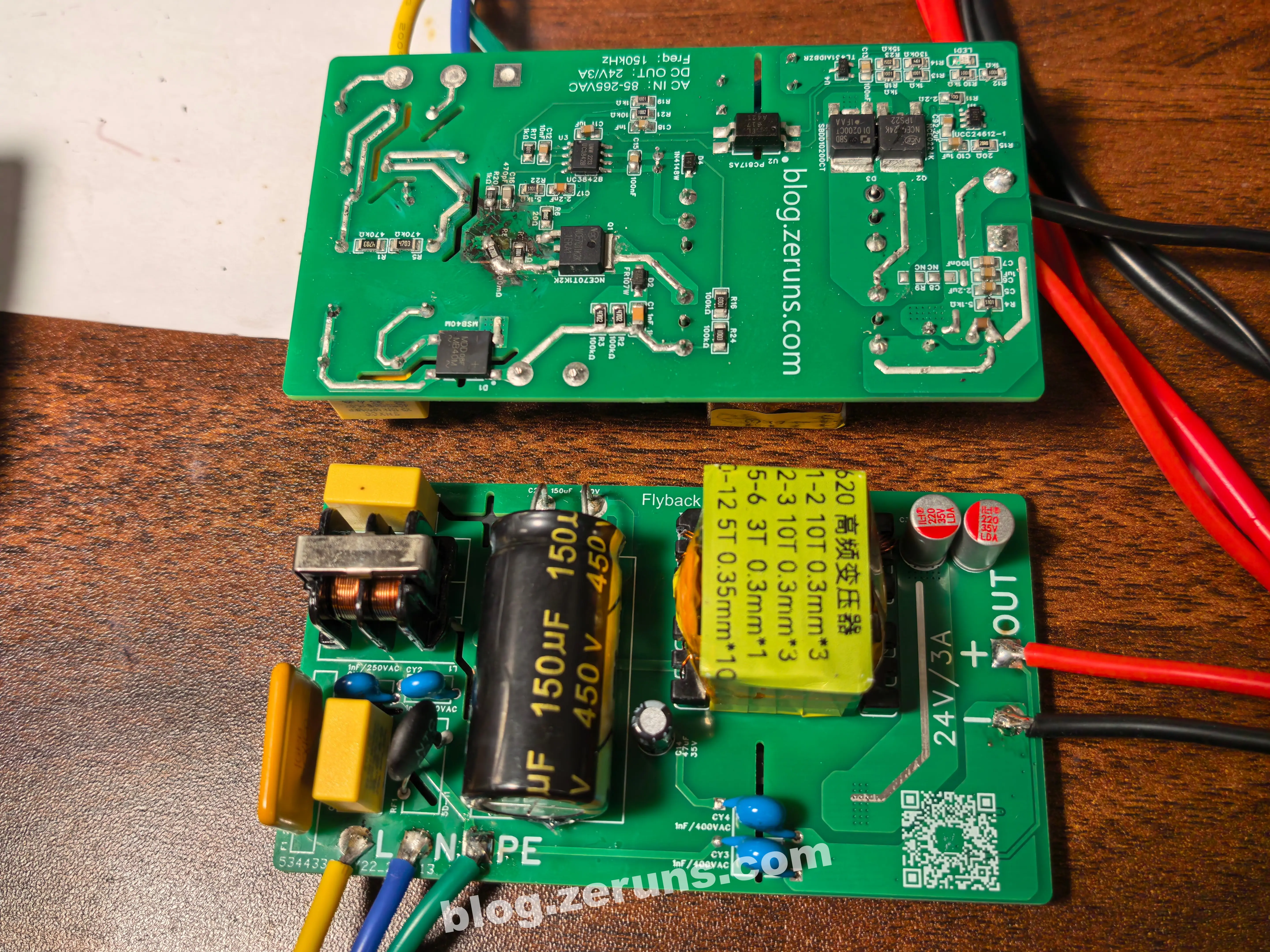
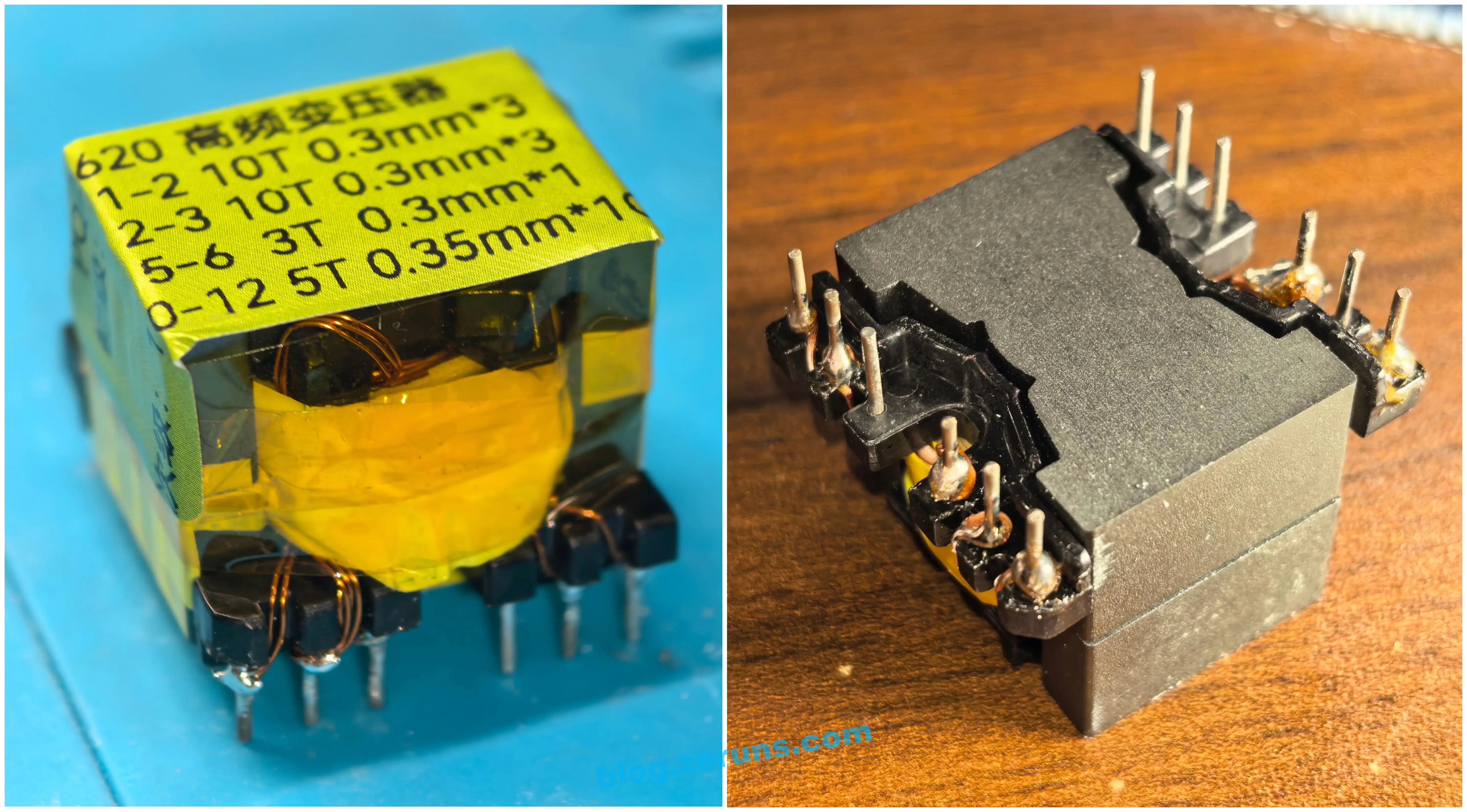
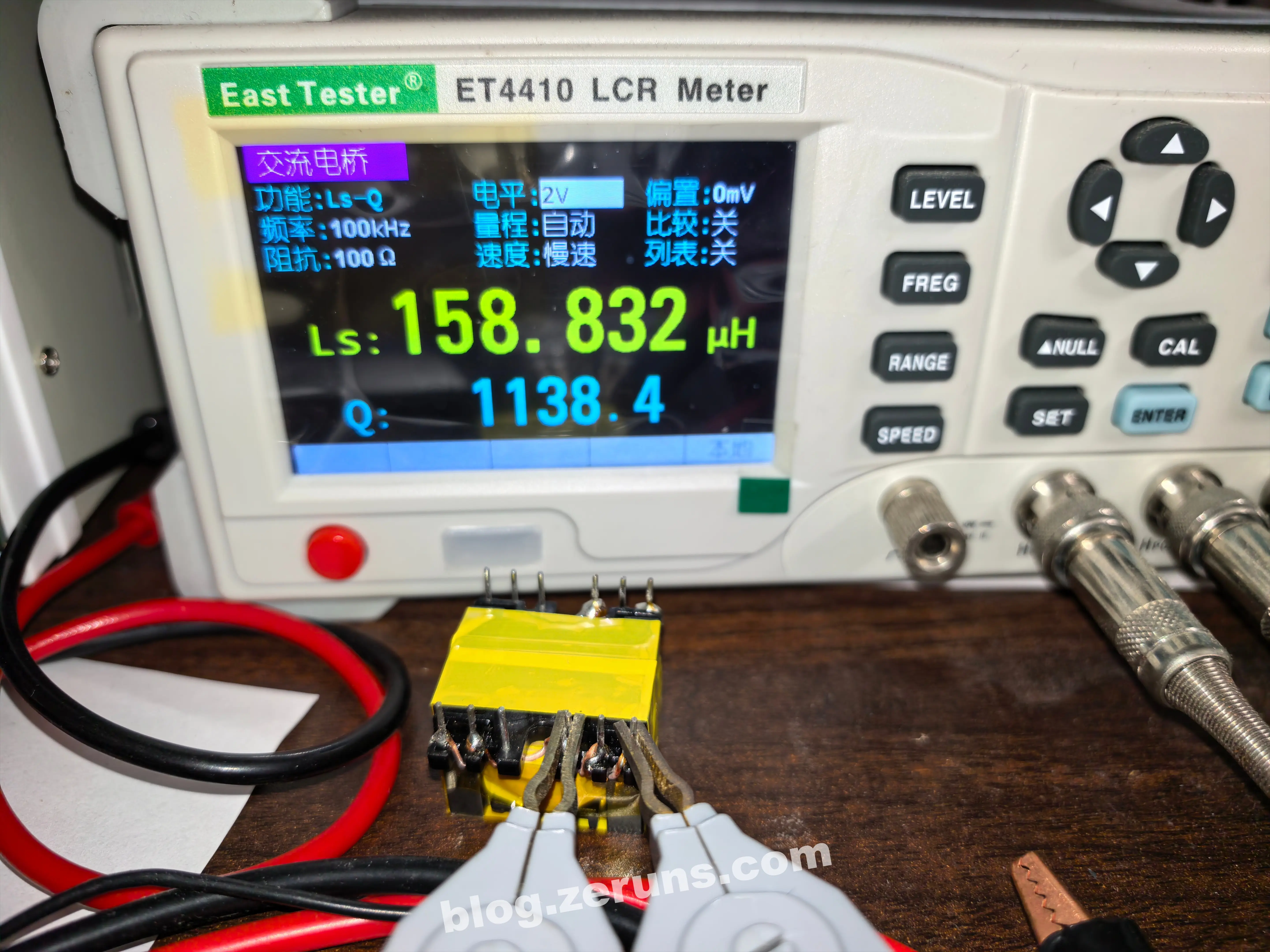
High-frequency transformer:
Testing and Performance Measurements
Initial Power-Up Test
During initial power-up testing, always connect a series incandescent bulb to limit current and prevent catastrophic failures in case of short circuits. The prototype worked as expected, producing an output voltage of 24.1V (tested under 0.9A load, shown below).
Purpose of the series light bulb: It acts as a current-limiting protective device. Under normal operation, the bulb’s resistance is low, so it only glows dimly or remains off, allowing normal testing. If a short circuit occurs inside the power supply, the current spikes, causing the bulb to drop most of the voltage due to its fixed resistance, thereby limiting current and protecting sensitive components from damage.
Switching power supply protection socket with built-in bulb: https://s.click.taobao.com/OiMyz3q
Alternatively, you can test using DC input. I verified that applying 60V DC allows the power supply to start up normally and output 24V. However, you must reduce the 200kΩ startup resistor (R24 + R16) to 100kΩ (by shorting one of them), otherwise the high resistance prevents startup at lower voltages.
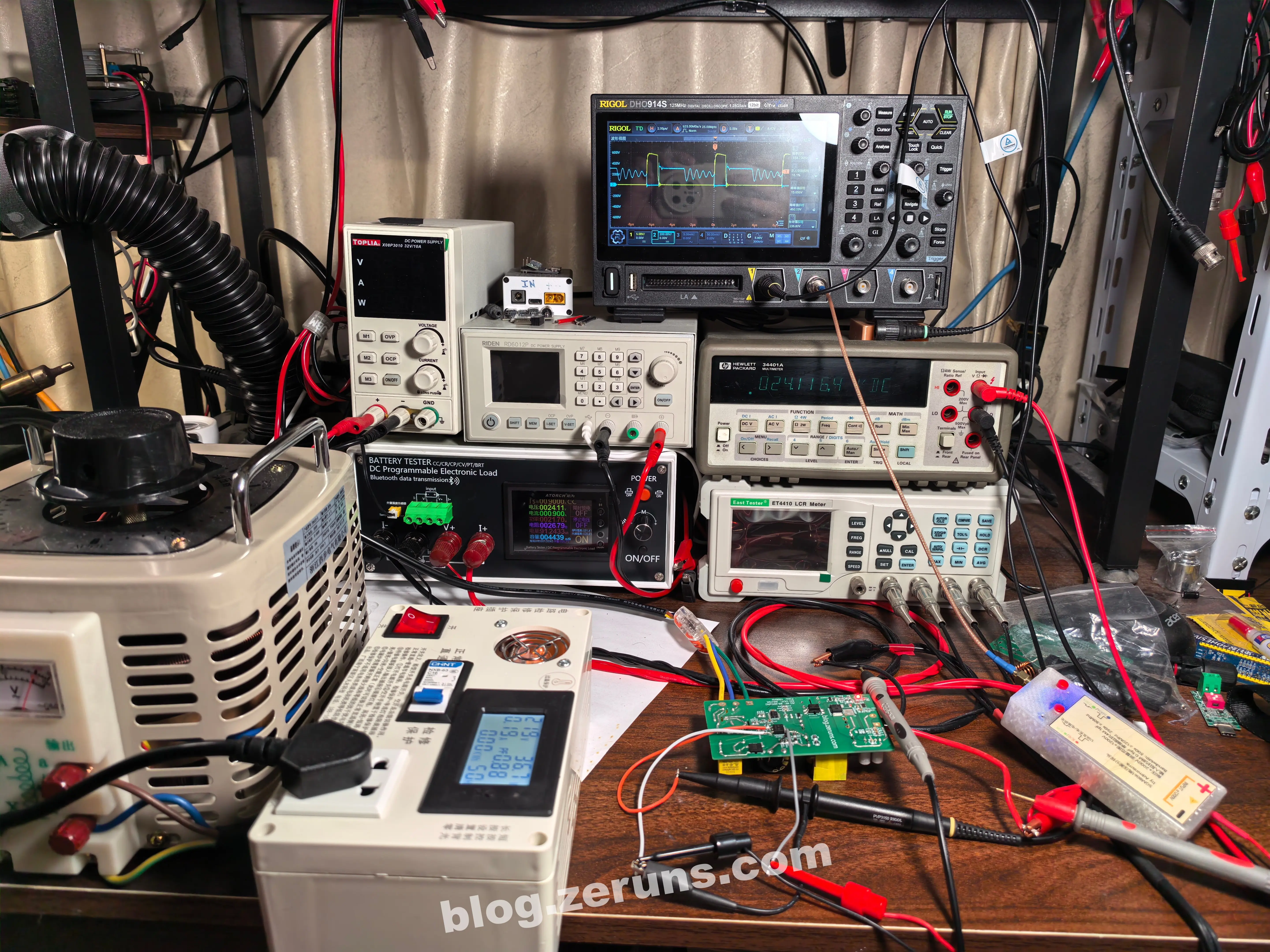
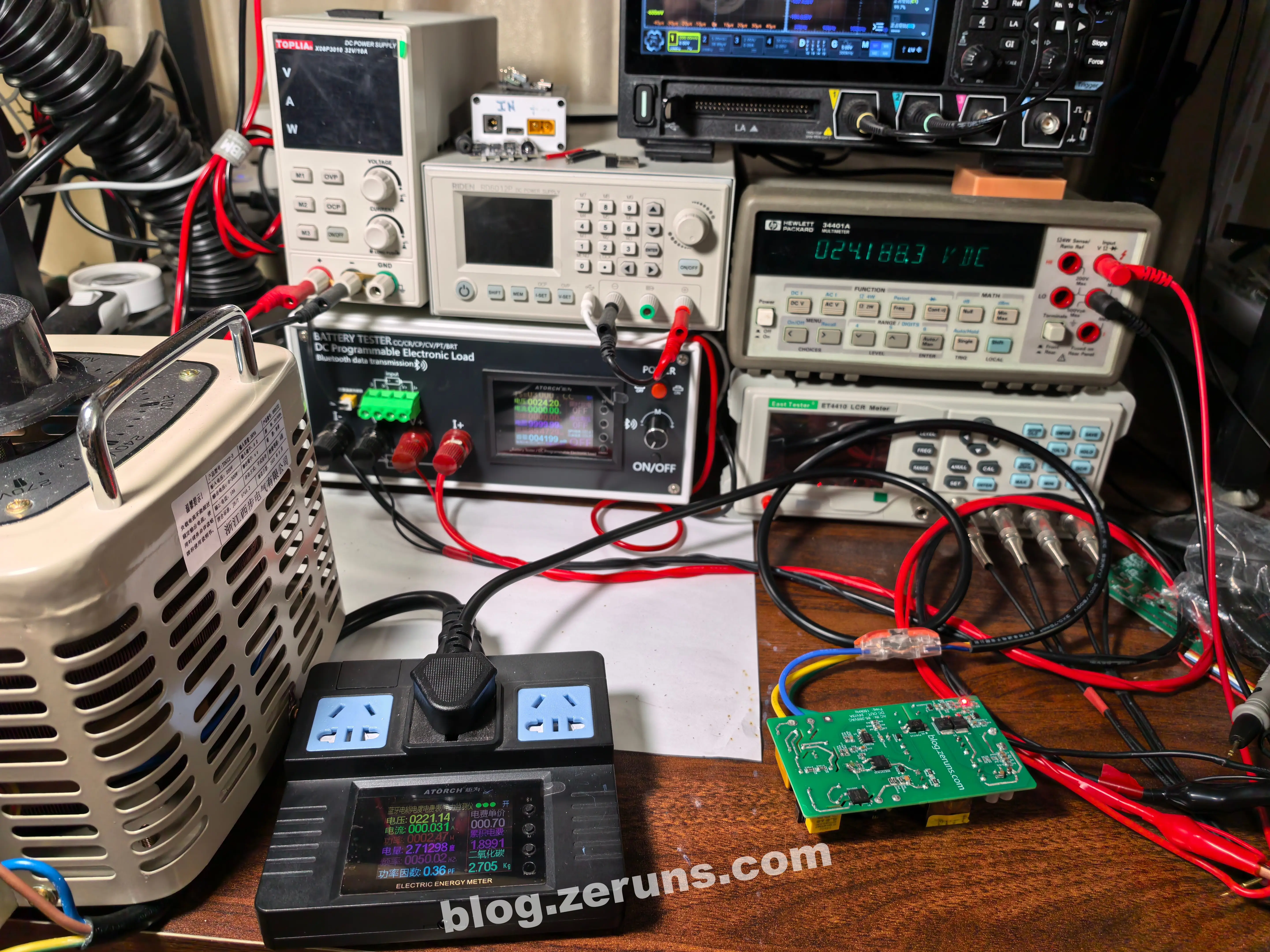
Efficiency Measurement
Test Equipment Used:
- Juwei Power Analyzer: https://u.jd.com/0gXabte
- Juwei Electronic Load: https://s.click.taobao.com/DvbzQ4q
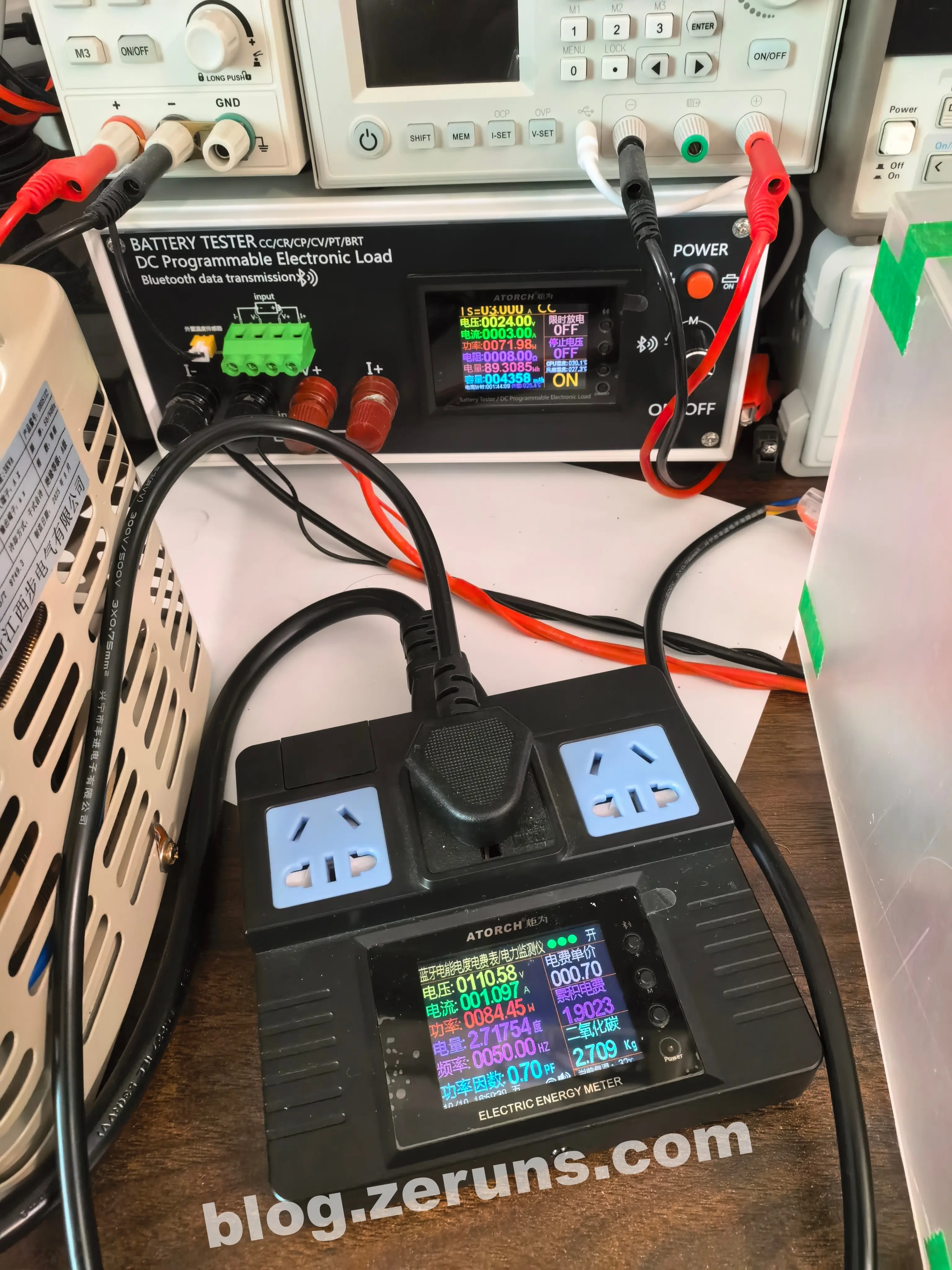
Measured Data:
| Input Voltage (V) | Input Current (A) | Apparent Input Power (W) | Active Input Power (W) | Output Voltage (V) | Output Current (A) | Output Power (W) | Efficiency (%) | Power Factor |
|---|---|---|---|---|---|---|---|---|
| 219.85 | 0.029 | 6.38 | 2.10 | 24.13 | 0.00 | — | — | 0.33 |
| 219.83 | 0.251 | 55.18 | 28.69 | 24.10 | 1.00 | 24.10 | 83.99 | 0.52 |
| 219.59 | 0.438 | 96.18 | 55.78 | 24.07 | 2.00 | 48.14 | 86.30 | 0.58 |
| 219.65 | 0.637 | 139.92 | 82.55 | 24.05 | 3.00 | 72.15 | 87.40 | 0.59 |
| 111.55 | 0.036 | 4.02 | 1.81 | 24.13 | 0.00 | — | — | 0.45 |
| 111.13 | 0.406 | 45.12 | 28.88 | 24.10 | 1.00 | 24.10 | 83.46 | 0.64 |
| 110.89 | 0.753 | 83.50 | 56.78 | 24.06 | 2.00 | 48.12 | 84.75 | 0.68 |
| 110.58 | 1.097 | 121.31 | 84.91 | 24.00 | 3.00 | 72.00 | 84.79 | 0.70 |
Peak measured efficiency: 87.4%, with minimum no-load power consumption of 1.81W — slightly higher than ideal.
The above efficiency measurements were taken using diode rectification, not synchronous rectification, because the selected synchronous rectifier MOSFET had relatively high on-resistance, resulting in lower efficiency compared to diode rectification. You may replace it with a better MOSFET for testing — choose one rated for at least 200V breakdown voltage (or 150V if snubber resistors R9 and capacitors C8, each 20Ω and 2.2nF, are added across the diode).
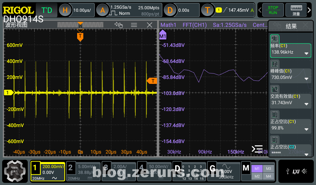
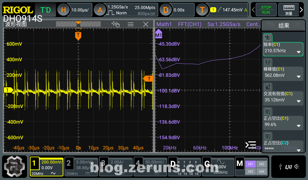
Output Voltage Ripple Measurement
Oscilloscope used: Rigol DHO914S: https://blog.zeruns.com/archives/764.html
The oscilloscope probe was clipped onto approximately 15cm of output wiring, without using a ground spring or connecting directly across the output capacitor. As such, the measured ripple values may be somewhat inflated.
Ripple at no load: Peak-to-peak ~730mV, ripple frequency ~138.96kHz (close to switching frequency).
Ripple under 3A load: Peak-to-peak ~562.08mV.
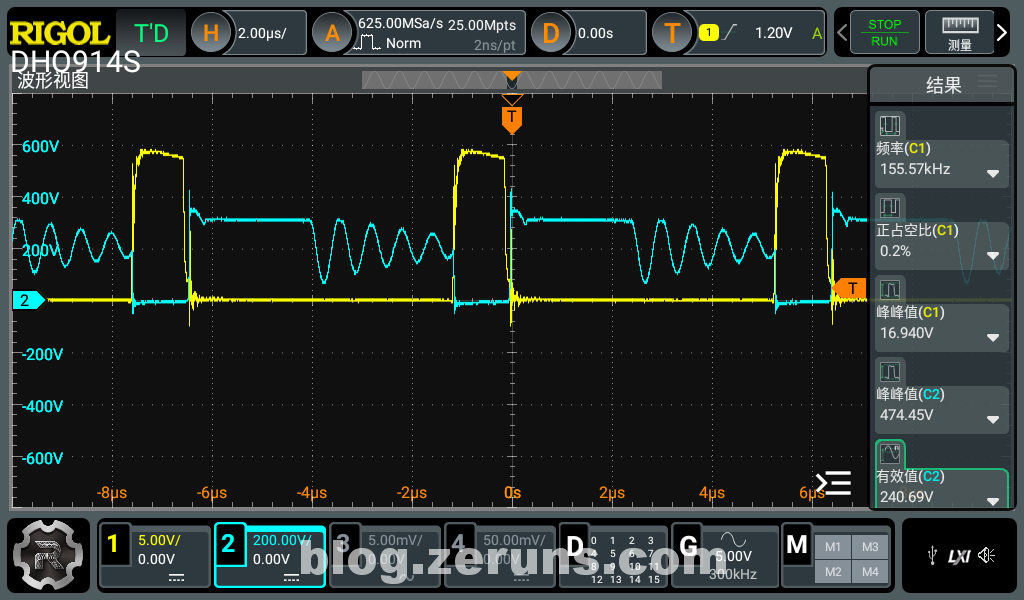
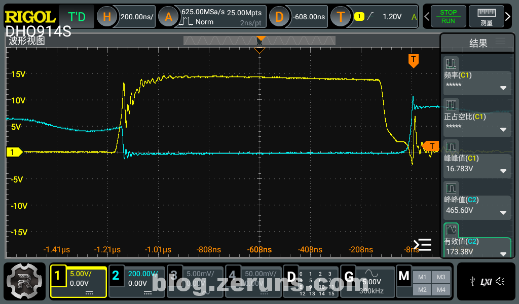
MOSFET Waveforms
Primary-side MOSFET gate-source (GS) and drain-source (DS) voltage waveforms with 220V AC input and 24V output under 1A load. Yellow trace = gate-to-source voltage; Blue trace = drain-to-source voltage.
Note that the drain voltage spike during turn-off reaches ~440V (measurement was taken with the series bulb still connected — forgot to bypass the switch — so actual input voltage might have been only ~100+ V, meaning the real spike could be even higher).
Zoomed-in view of gate voltage waveform:
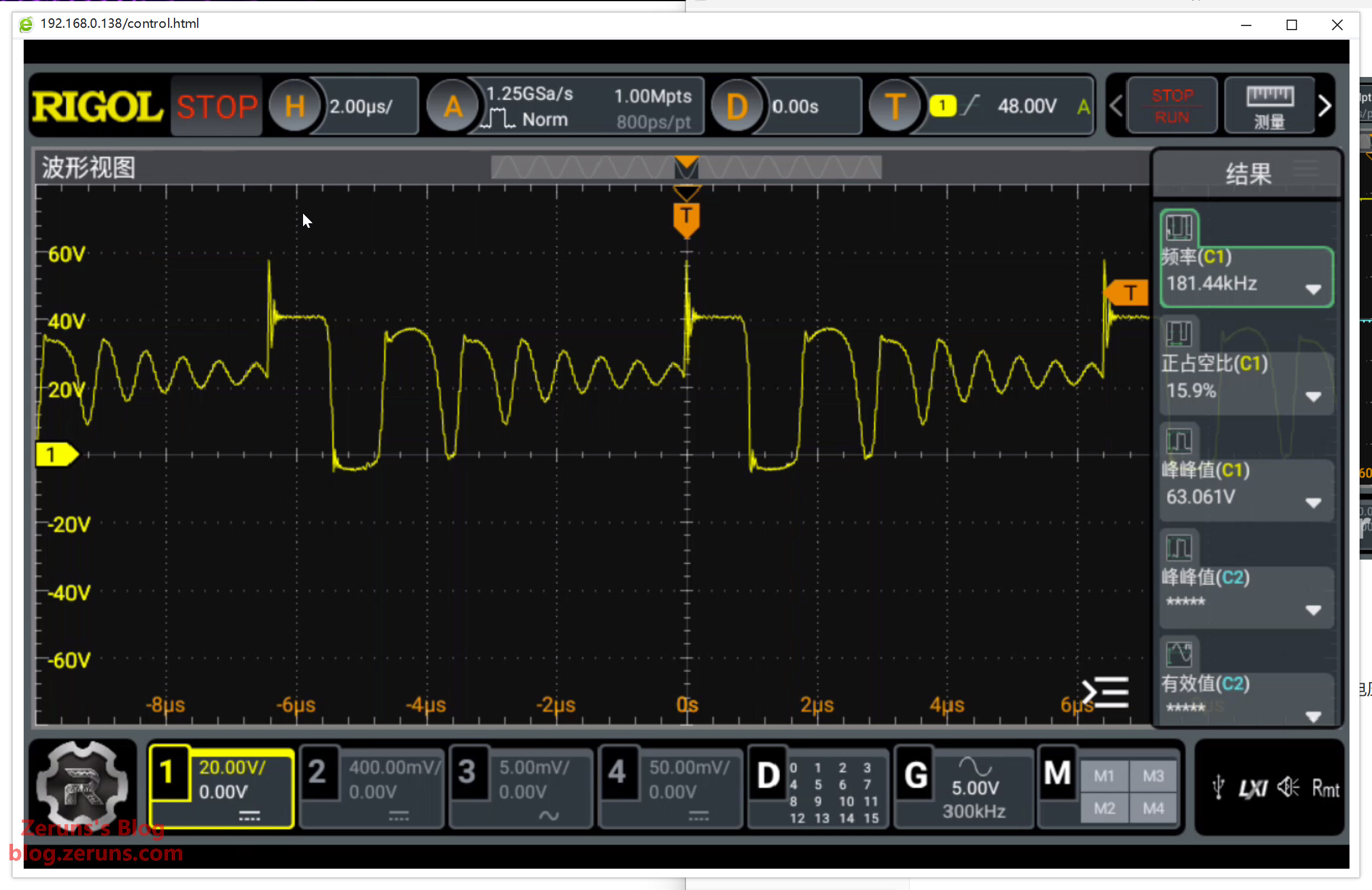
Output Rectifier Diode Waveforms
Output rectifier voltage waveform with 60V DC input, 24V output, no load — peak voltage spike ~56V.
(After adding 20Ω resistor R9 and 2.2nF capacitor C8 across the diode, spike drops to ~42V)
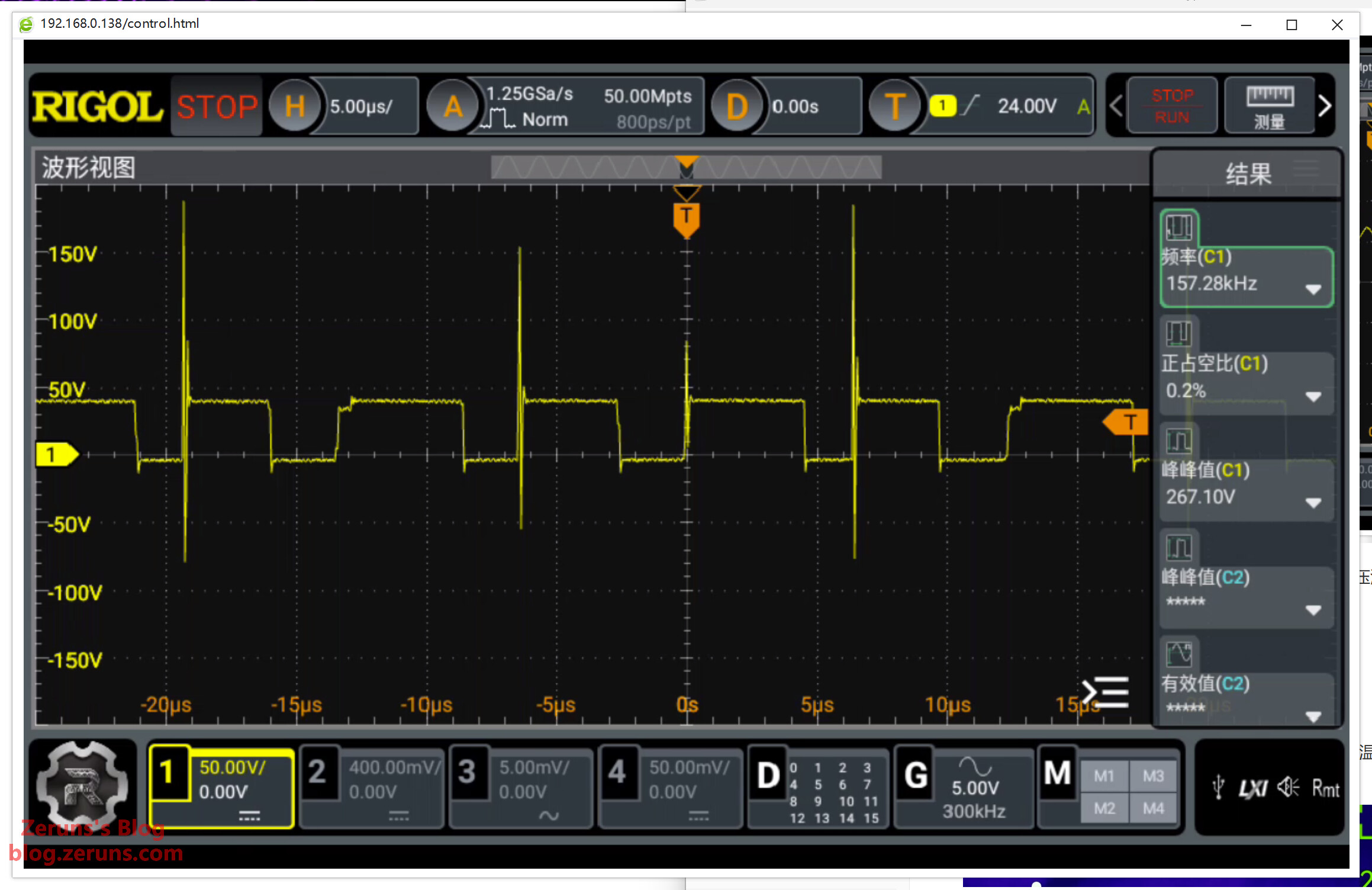
With 60V DC input, 24V output, 1A load — peak voltage spike ~190V.
(After adding R9 and C8, spike reduces to ~81V)
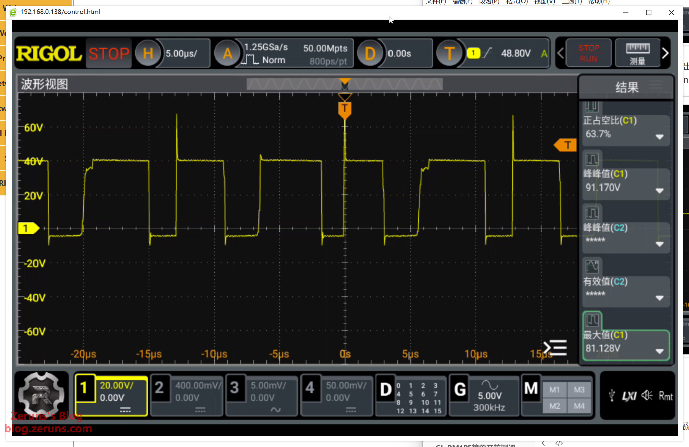
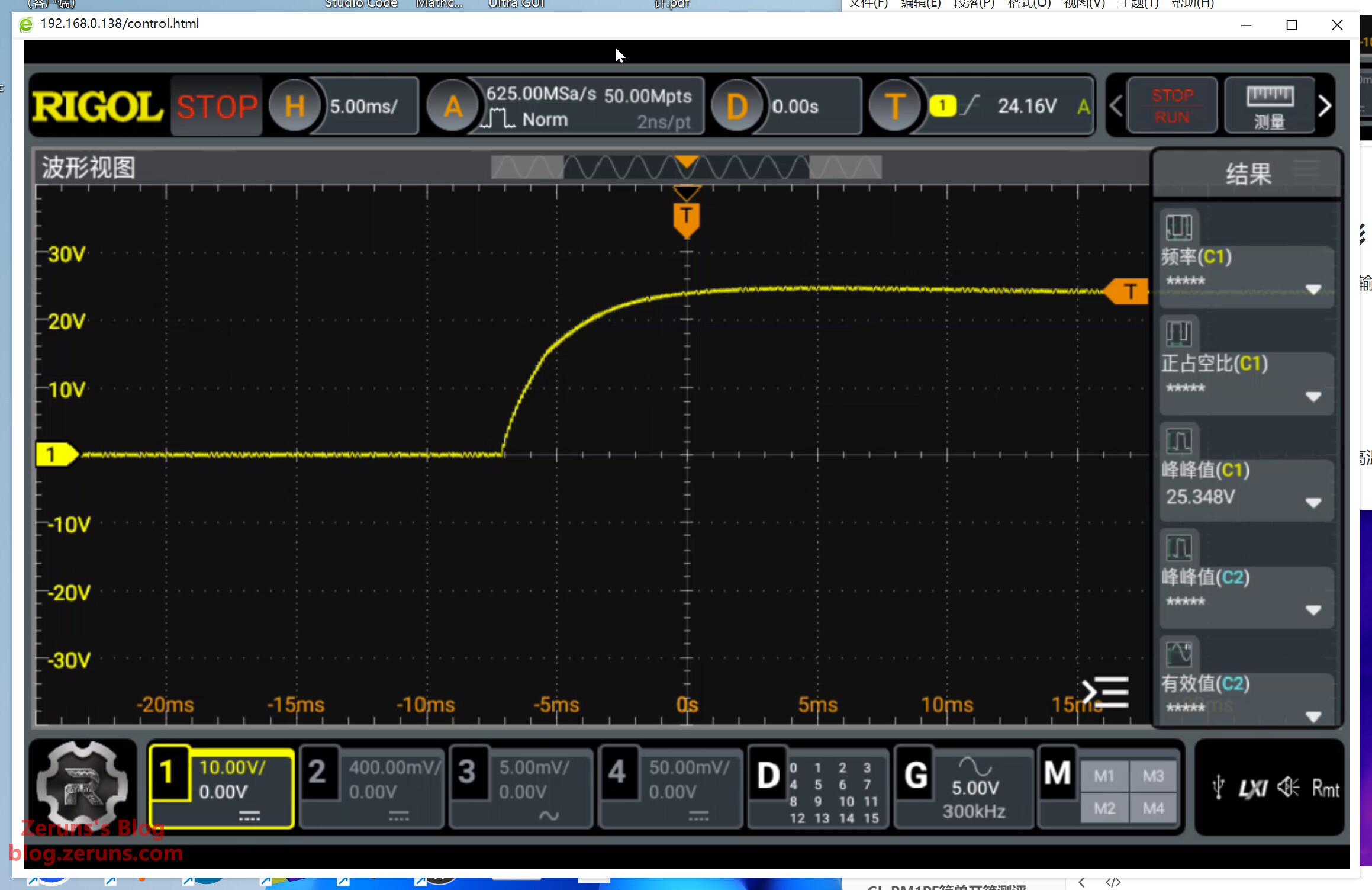
No-Load Startup Output Voltage
Output voltage waveform during startup with 60V DC input, 24V output, no load. Rise time from 0V to 24V is about 7 milliseconds.
Thermal Performance
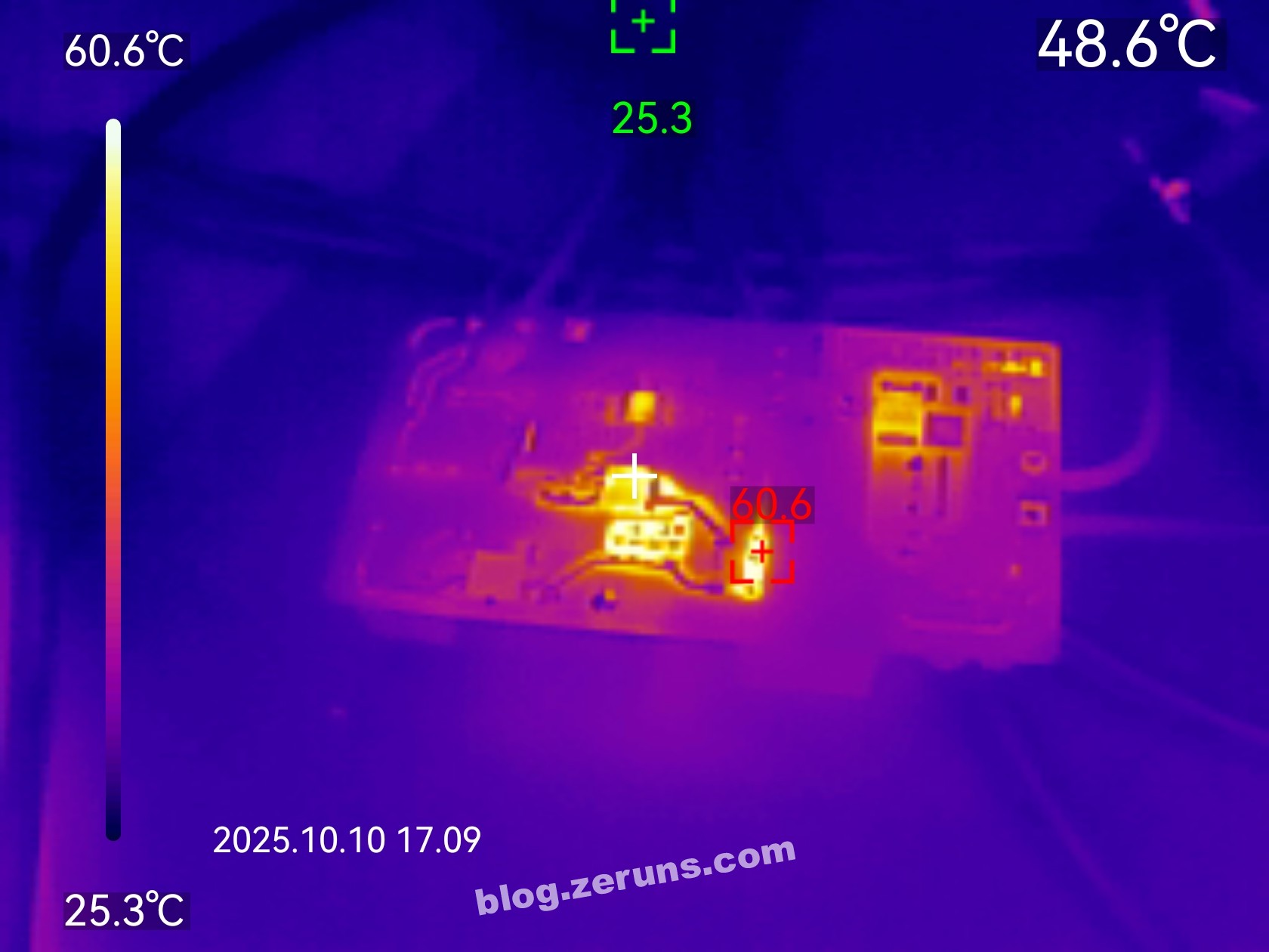
Thermal imaging of the bottom side under no load: Highest temperature (~60°C) observed at the startup resistor (ambient ~25°C), primary-side MOSFET ~48°C.
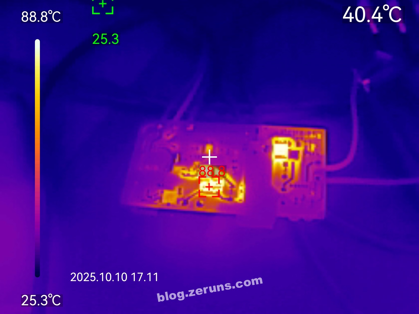
Thermal imaging under 3A full load: Hottest spot (>88°C) located at either the primary-side MOSFET or the resistor in the RCD clamp circuit (ambient ~26°C). Secondary-side rectifier diode likely exceeds 60°C.
Temperature is quite high under full load. For long-term full-power operation, the primary-side switch MOSFET should be fitted with a heatsink or potted (encapsulated) to transfer heat to the enclosure!
Component Purchase Links- SMD resistor and capacitor sample book: https://s.click.taobao.com/ngH2RGq
- PQ transformer core and bobbin: https://s.click.taobao.com/EJtb04q
- UC3842 chip: https://s.click.taobao.com/7pfvQGq
- PC817A optocoupler: https://s.click.taobao.com/Le1X04q
- MSB40M rectifier bridge: https://s.click.taobao.com/7HqQQGq
- SBDD10200CT diode: https://s.click.taobao.com/izw104q
- UCC24612-1 synchronous rectification controller: https://s.click.taobao.com/K1gEQGq
- TL431 voltage reference: https://s.click.taobao.com/DPxnz3q
- UU10.5 common mode choke: https://s.click.taobao.com/D1t1z3q
- 5D-11 thermistor: https://s.click.taobao.com/IsOry3q- Safety Capacitor X2: https://s.click.taobao.com/vBeCPGq
- Safety Y Capacitor: https://s.click.taobao.com/sas5PGq
It is recommended to purchase components from LCSC (SZLCSC Mall): https://activity.szlcsc.com/invite/D03E5B9CEAAE70A4.html
In the BOM list of the open-source link on LCSC, click “Order Now” to import all required components directly into your shopping cart with one click.
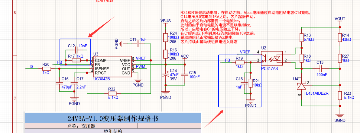
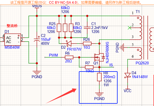
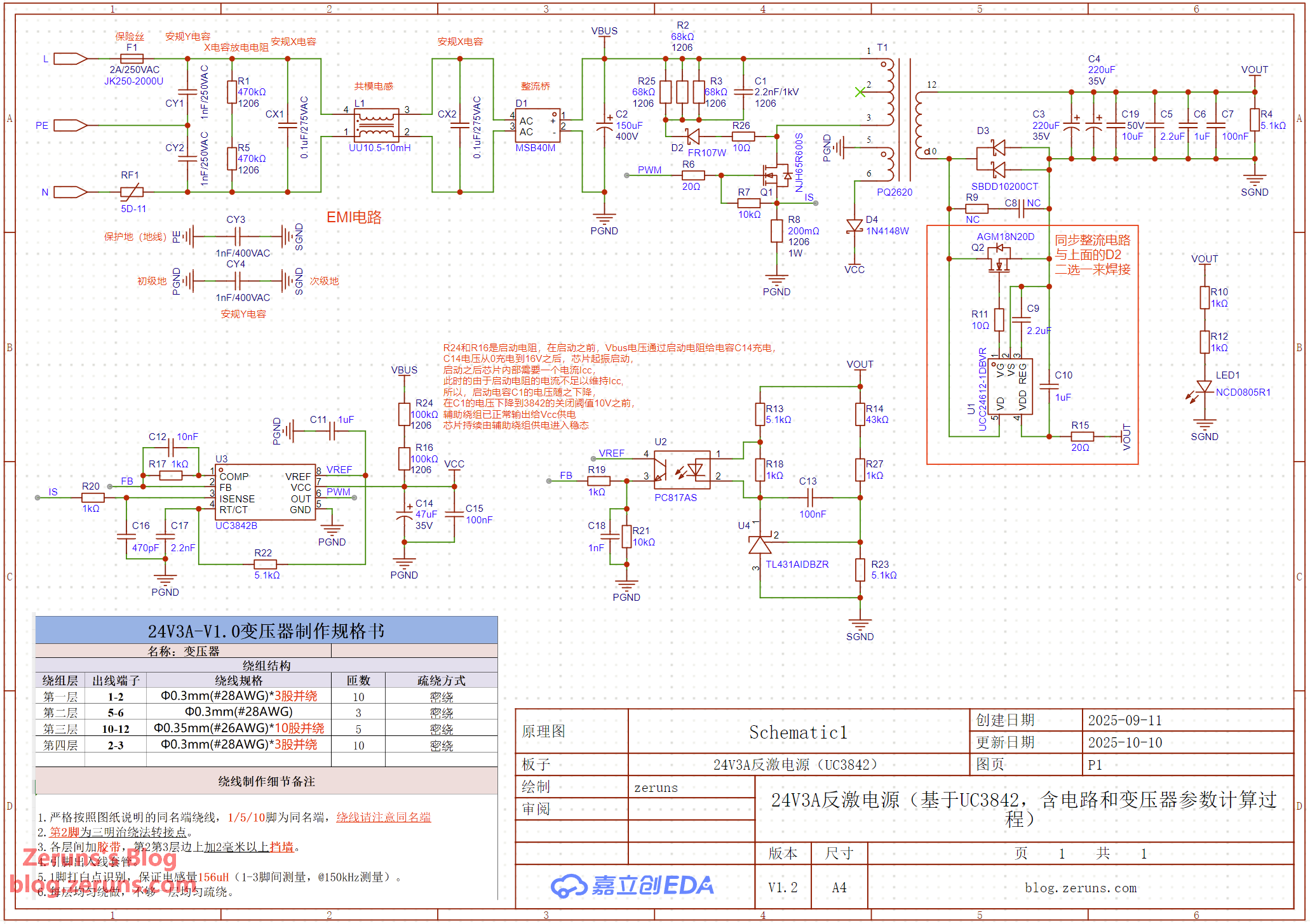
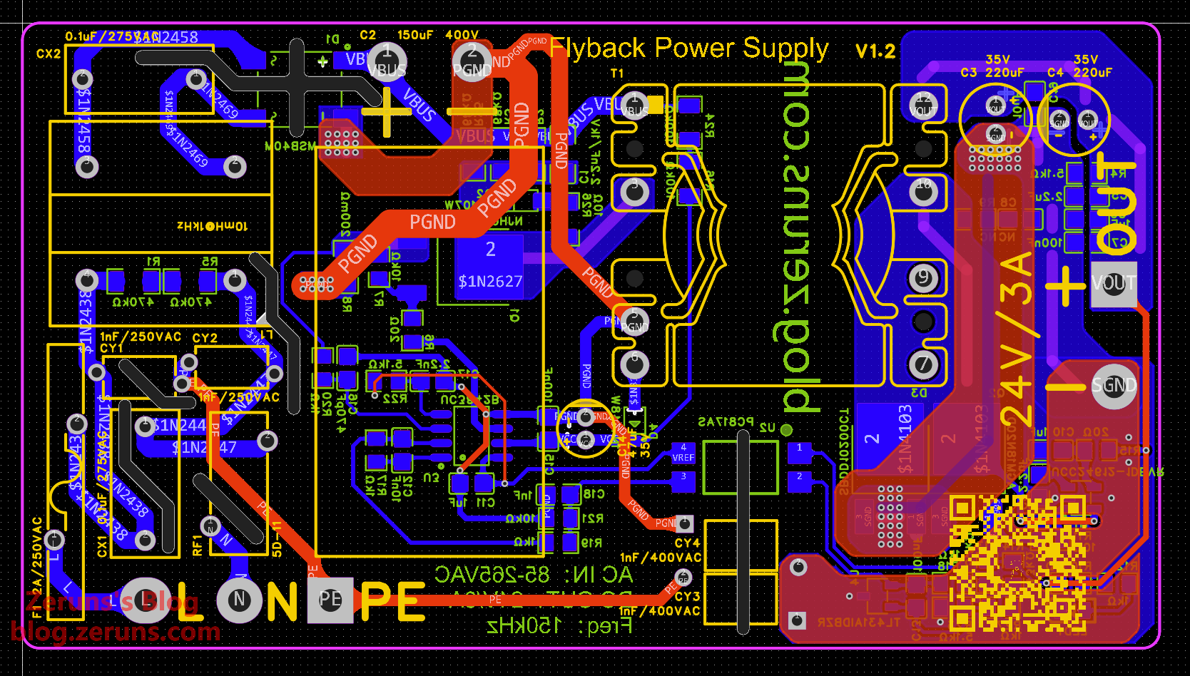
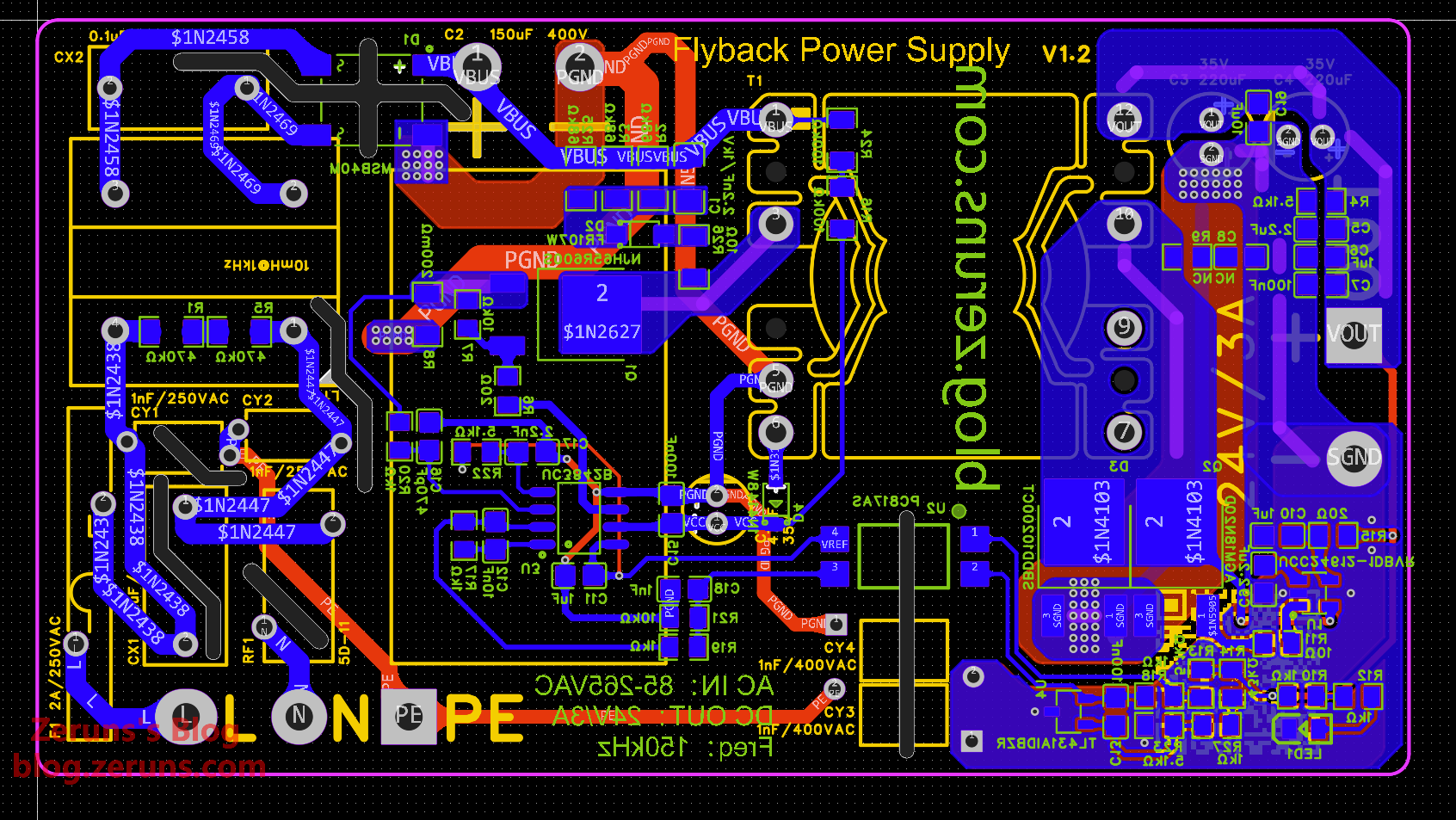
Schematic Diagram
PCB Layout
Top Layer
Bottom Layer
Download Resources
The following links contain resources such as: LCEDA project files, schematic PDFs, Gerber files for PCB fabrication, SMPSKit switching power supply design tool, flyback transformer calculation sheet (Mathcad), silkscreen diagrams, transformer manufacturing specifications, datasheets for all ICs, PSIM simulation models, Bode plot MATLAB code, and other reference materials and documents. (Some materials are collected from the internet.)
- 123 Cloud Pan: https://www.123684.com/s/2Y9Djv-2hTdH
- Baidu Netdisk: https://pan.baidu.com/s/1767xJthTFWQbxgeZQXM_Hg?pwd=9527 Password: 9527
If you find this helpful, feel free to support me via donation through the 123 Cloud Pan link above. If reading this article on WeChat (Official Account: zeruns-gzh), you can also tap “Like Author” at the bottom of the article to donate. Thank you.
Recommended Open Source Projects
- Three-phase Power Meter – Open Source Project (help monitor home electricity usage): https://blog.zeruns.com/archives/771.html
- STM32-based Synchronous Rectifier Buck-Boost Digital Power Supply – Open Source: https://blog.zeruns.com/archives/791.html
- LM25118 Automatic Buck-Boost Adjustable DCDC Power Module: https://blog.zeruns.com/archives/727.html
- Smart Electronic Load Based on CH32V307 – Open Source (Embedded Competition Entry): https://blog.zeruns.com/archives/785.html
- EG1151 High-Power Synchronous Rectifier Adjustable Buck-Boost Power Module (Supports Type-C PD Fast Charging Input) – Open Source: https://blog.zeruns.com/archives/794.html
- Open Source 140W+65W Buck-Boost PD3.1 Fast Charging Module (2C+1A Ports), IP6557+IP6538, 205W Desktop Charger: https://blog.zeruns.com/archives/801.html
- Open Source Type-C Docking Station with 4× 10Gbps USB-A Ports + 2.5G Ethernet + Card Reader: https://blog.zeruns.com/archives/868.html
Recommended Reading
- Affordable and High-Performance VPS / Cloud Servers Recommendation: https://blog.zeruns.com/archives/383.html
- Minecraft Server Hosting Guide: https://blog.zeruns.com/tag/mc/
- Guide to Building Cross-border E-commerce Independent Websites – WordPress International Website Setup: https://blog.zeruns.com/archives/889.html
- ZGRL-80 Photography Light Teardown and Circuit Design Analysis: https://blog.zeruns.com/archives/882.html
- Mechanical Revolution Code10AI Laptop (Ultra7-255H) – Initial Unboxing Review and Teardown: https://blog.zeruns.com/archives/895.html
- GL-RM1PE – Simple Unboxing Review and Teardown (Enables BMC Remote Management on Regular PCs): https://blog.zeruns.com/archives/900.html
English Version of the Article: https://blog.zeruns.top/archives/74.html