基于STM32G474的四开关Buck-Boost数字电源,支持Type-C接口PD诱骗输入和DC5.5接口输入,最大输入/输出48V10A。这是我的毕业设计,现已开源,包括原理图、PCB、程序源码、外壳3D模型等资料。
作品水平一般,轻喷。欢迎友好交流。
作品演示视频:https://www.bilibili.com/video/BV1Ui421y7ip/
基于CH32V307的智能电子负载开源,嵌入式设计大赛作品:https://blog.zeruns.com/archives/785.html
本项目在立创开源平台的开源链接:https://url.zeruns.com/noGf0
电子/单片机技术交流QQ群:2169025065
资料下载链接在文章末尾。
硬件电路使用立创EDA设计,确实很好用。
简介
本文设计了一款基于STM32的同步整流Buck-Boost数字电源。该电源电路由MOSFET驱动电路、4开关Buck-Boost电路、信号调理电路、PD快充协议电路、辅助电源电路、单片机控制电路等部分组成。
该电源可通过DC接口或Type-C接口供电,Type-C接口支持与充电器通过PD快充协议通信,自动申请获取最高20V工作电压。电源采用STM32G474单片机实时监测输入输出电压电流,通过PID控制算法调节输出PWM占空比,实现过压过流保护,还可采样主板温度实现过温保护。此外,可通过OLED屏查看电源实时参数,通过旋转编码器和按键设置输出电压电流,还可通过另一个Type-C接口与上位机通信,通过上位机软件查看电源实时参数和波形。
设计性能参数
电源的设计性能参数如下:
| 项目 | 参数指标 |
|---|---|
| 输入电压范围 | 12Vdc~48Vdc |
| 输入电流范围 | 0~10A |
| 最大输出功率 | 450W |
| 输出电压范围 | 0.5Vdc~48Vdc |
| 输出电流范围 | 0~10A |
| 输出电压纹波 | 峰峰值 ≤ 200mV |
| 开关频率 | 181.333kHz |
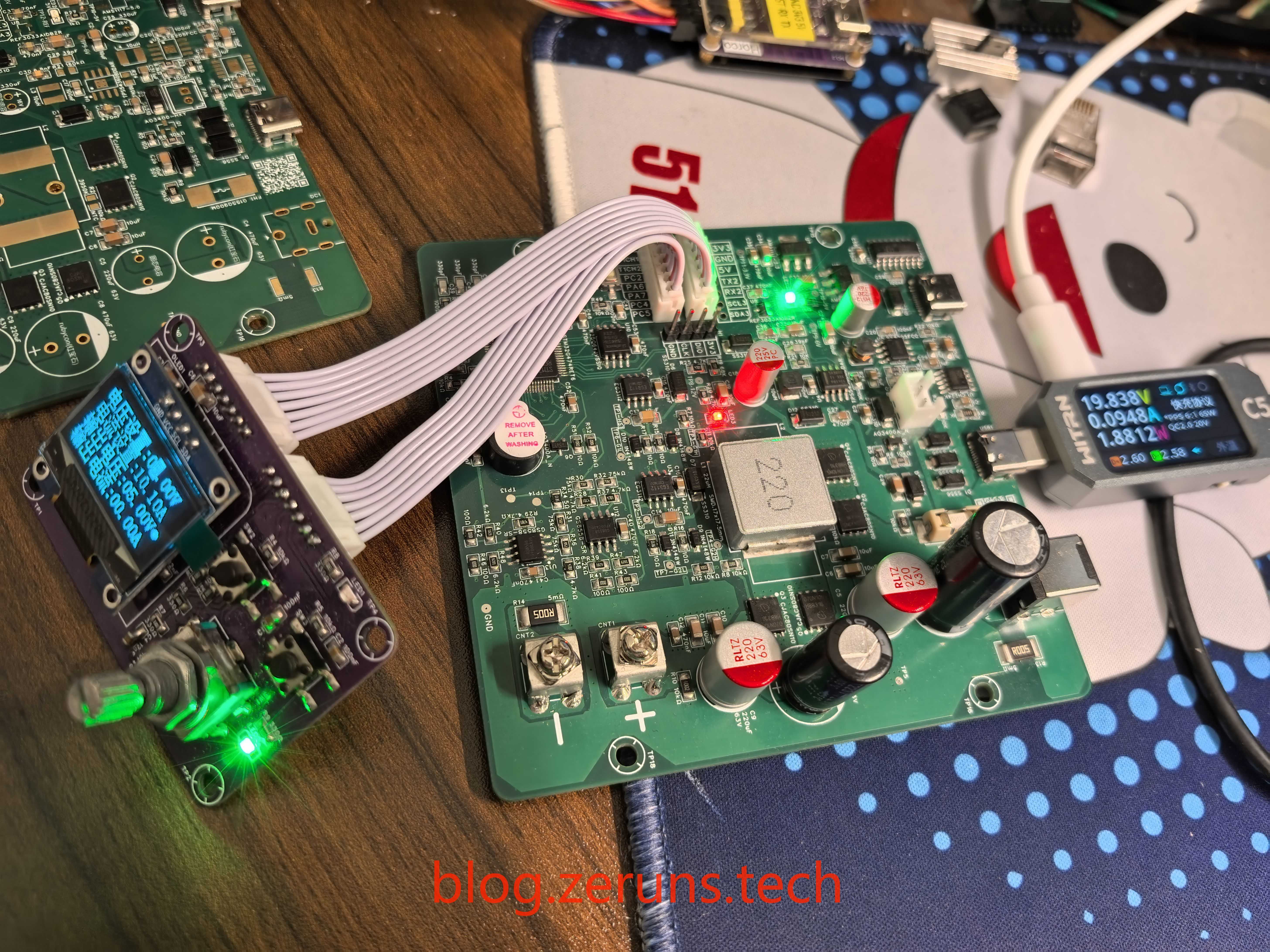
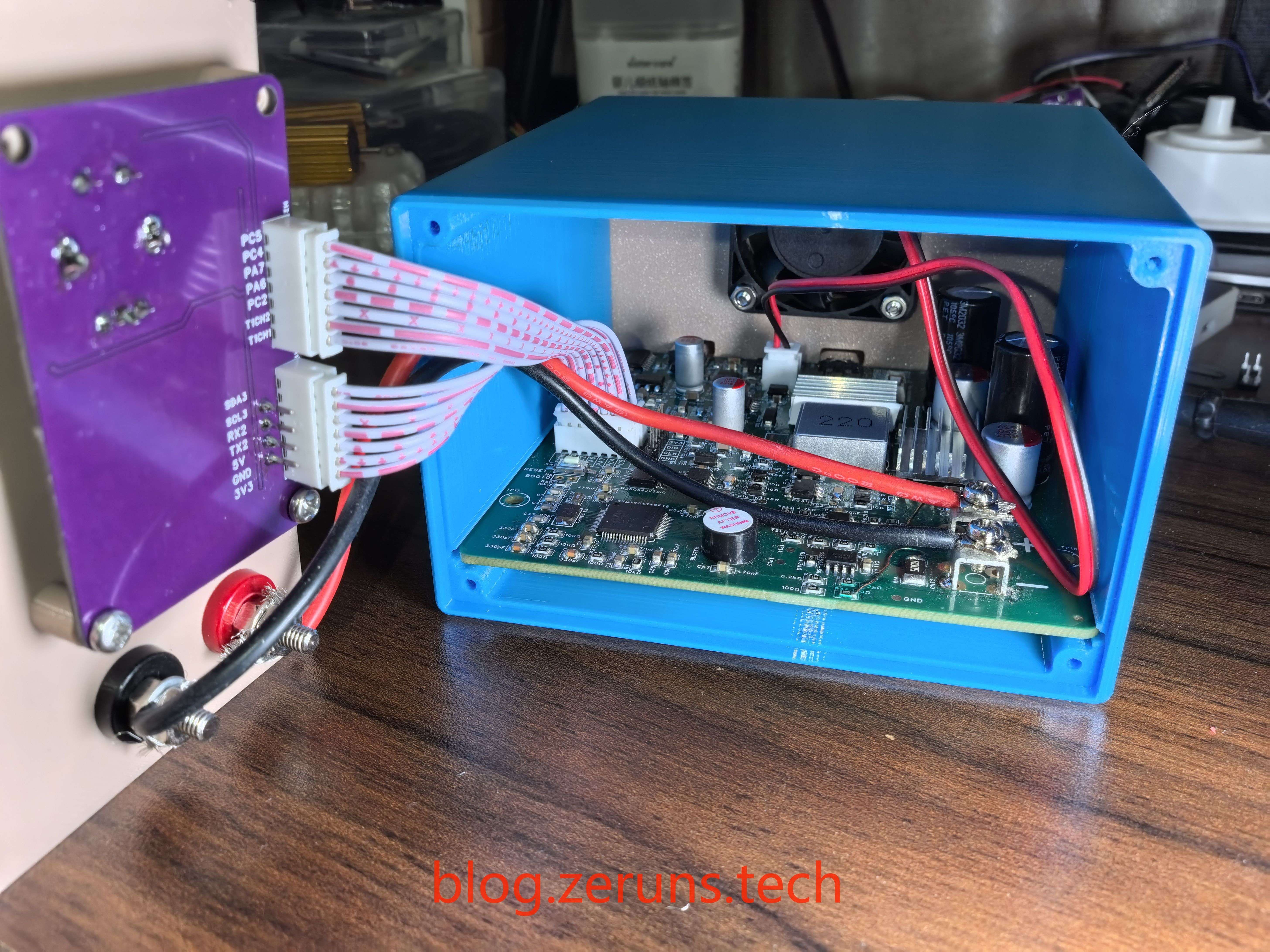
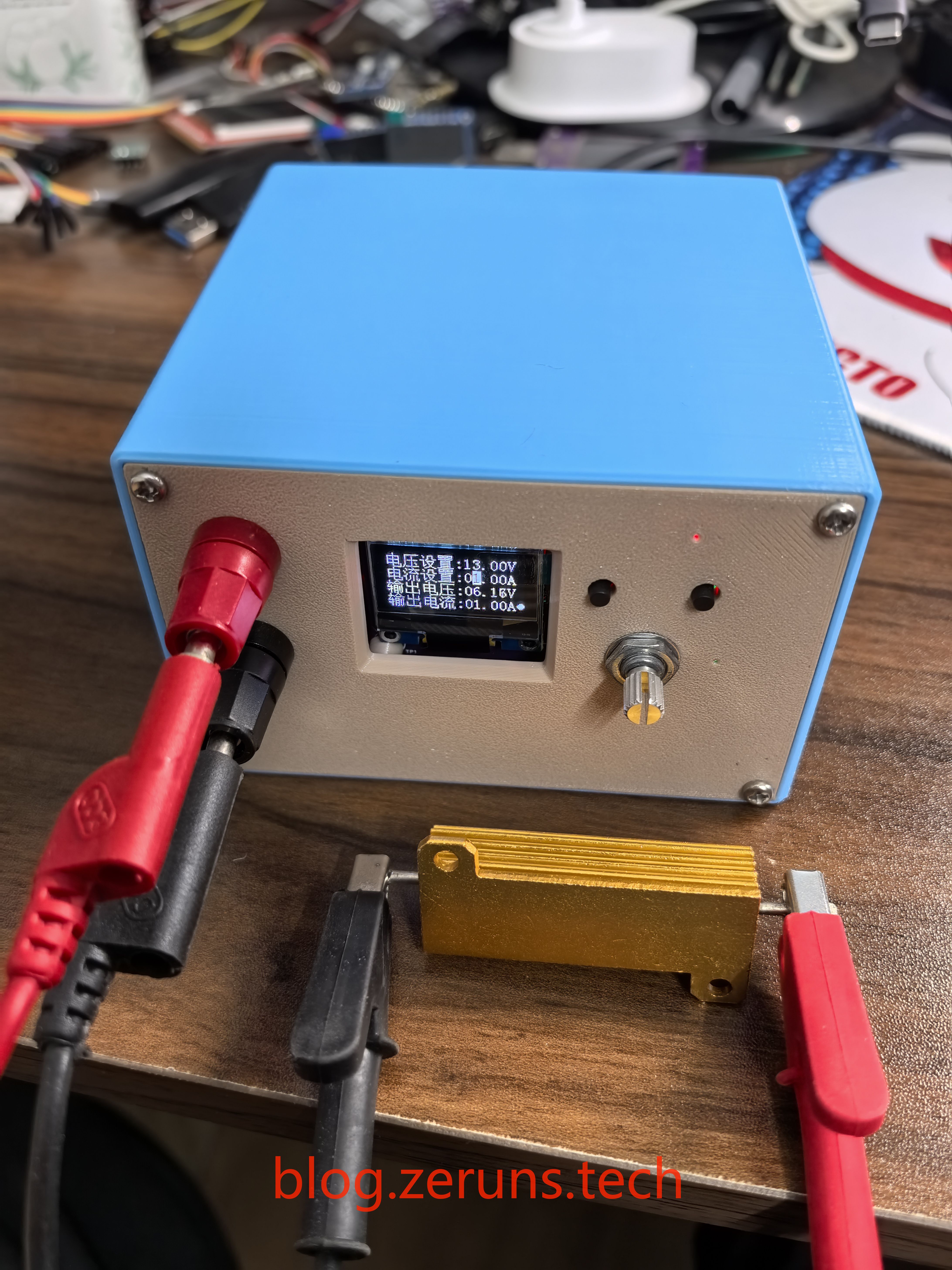
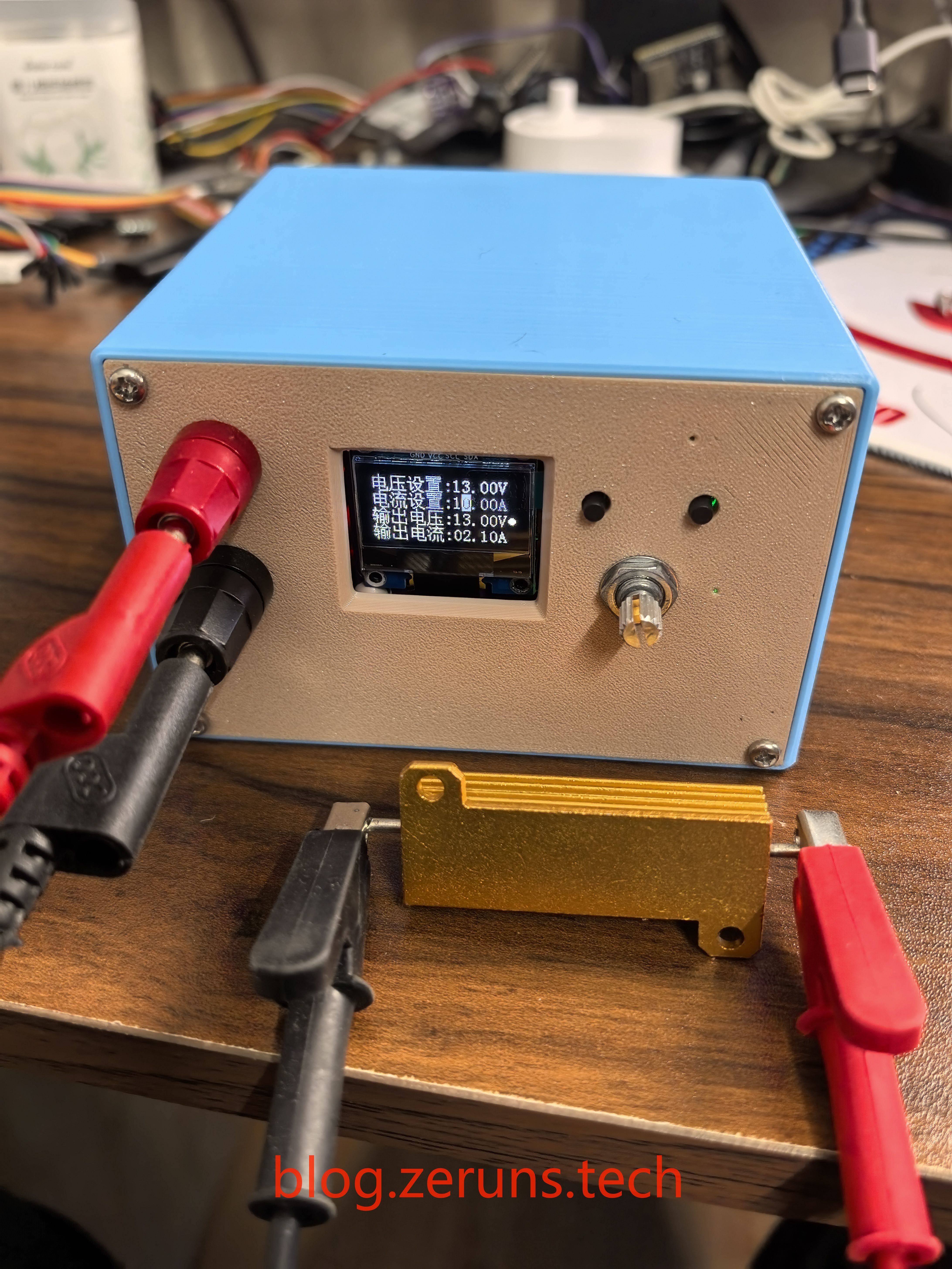
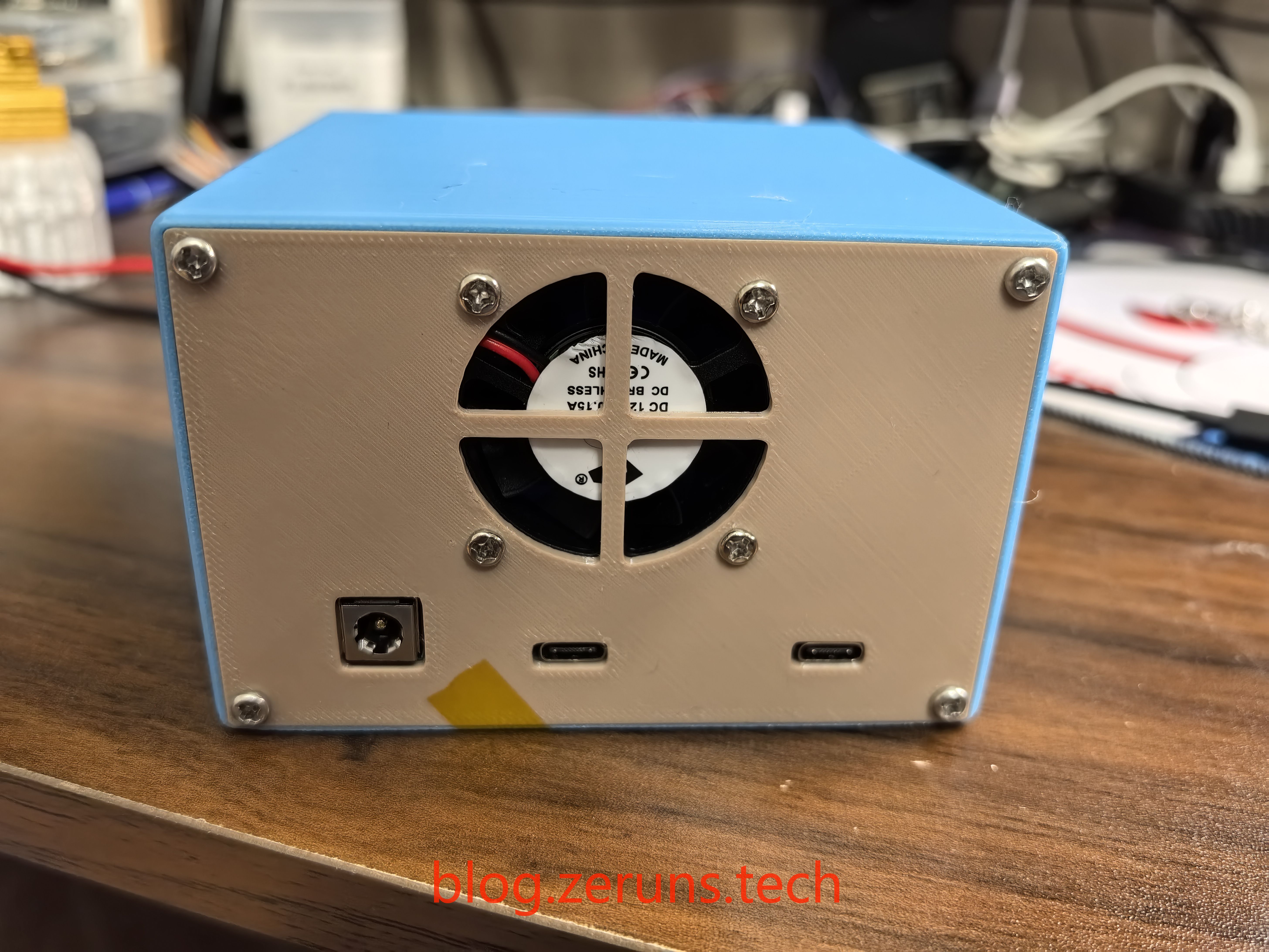
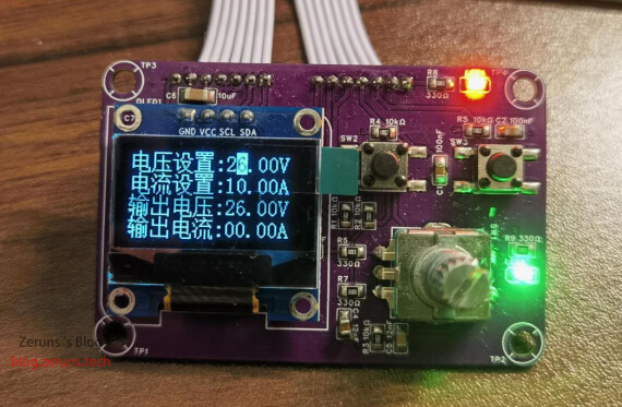
实物图片
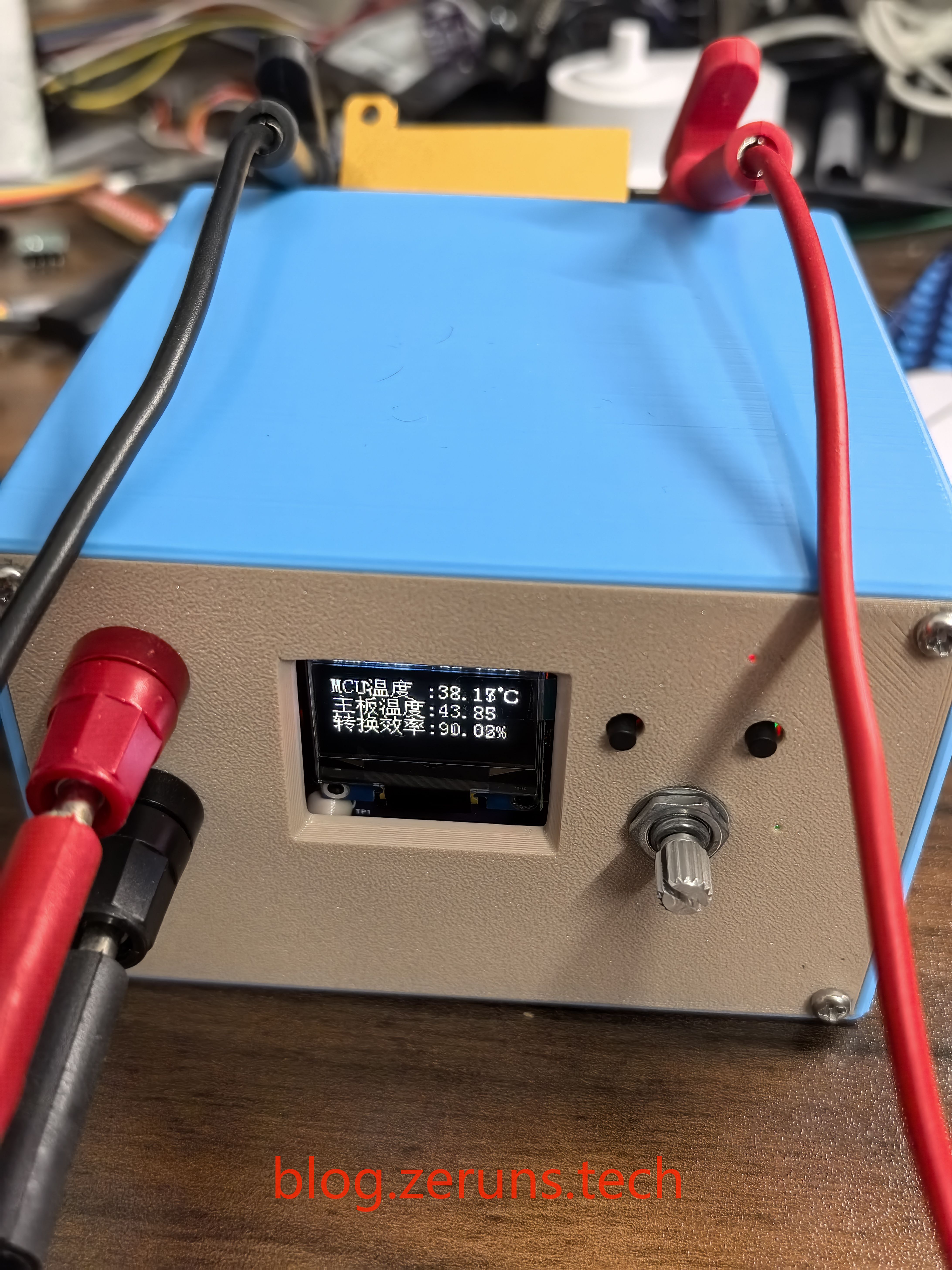
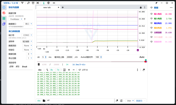
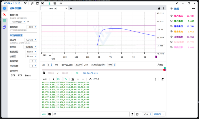
上位机软件使用VOFA+,可实时查看电源各项参数(输入电压电流、输出电压电流、主板温度、MCU温度、电源转换效率等)及波形变化,如下图所示。
系统框图

硬件电路设计
元件选型与计算
电感计算
在同步BUCK-BOOST电源中,电感计算需考虑BUCK模式与BOOST模式下的工作条件,以确保在两种模式下均能满足电路要求。通常,电感选择依据两种模式中对电感要求更高的模式进行。
当电源工作在BUCK降压模式时,假设最大输入电压为48V,最小输出电压为5V,计算最小PWM占空比:
$$\nD_{min} = \frac{V_{out\min}}{V{in\_max}} = \frac{5V}{48V} = 10.417\%\n$$
定义电感电流纹波(最大额定电流纹波的25%,设定最大额定电流为10A):
$$\n\Delta I_L = 25\% \cdot I_{out\_nom} = 25\% \times 10A = 2.5A\n$$
计算BUCK所需最小电感:
$$\nL_{minBuck} = \frac{V_{out\min} \cdot (1 - D{min})}{\Delta I_L \cdot f_{switch}}\n= \frac{5V}{2.5A \times 181333Hz} \times (1 - 10.417\%) \n\approx 9.88\mu H\n$$
当电源工作在BOOST升压模式时,取额定输入电压24V为计算点,计算PWM占空比:
$$\nD_{Bo} = 1 - \frac{V_{in\nom}}{V{out\_max}} = 1 - \frac{24V}{48V} = 50\%\n$$
在Boost模式下,取1A($I_{minb}$)时,Boost进入连续导通模式(CCM),计算电感:
$$\nL_{minBoost} = \frac{V_{out\max} \cdot D{Bo}(1-D_{Bo})^2}{2 \cdot I_{minb} \cdot f_{switch}} \n= \frac{48V \times 50\% \times (1 - 50\%)^2}{2 \times 1A \times 181333Hz} \n= 16.544\mu H\n$$
根据公式计算所得结果,确定满足预定纹波电流要求所需的最小电感值。为确保该条件得以满足,应选取电感值略高于计算值的电感器。同时,必须确保所选电感的饱和电流能够承载电路中最高的电流峰值。由于计算过程中未考虑效率因素,实际占空比与峰值电流可能低于理论计算值。因此,在进行选择时,应留有一定的安全裕量,以适应实际工况下可能出现的各种情况。
综合考虑上述因素,本设计选用22μH、1770贴片封装、饱和电流10A以上的电感作为BUCK-BOOST电路的电感元件。
电容计算
为获得良好的输出电压纹波,设计电压纹波为50mV。
$$\n\Delta V_{out} = 0.05V\n$$
上面所选电感为22μH,因此这里计算采用该电感值:
$$\nL_{BB}=22\mu H\n$$
分别计算在BUCK降压模式和BOOST升压模式工作时所需的最小电容$C_{minBuck}$和$C_{minBoost}$:
$$\nC_{minBuck}=\frac{V_{out\min}\cdot(1-\frac{V{out\min}}{V{in\max}})}{8\cdot L{BB}\cdot \Delta V_{out}\cdot {f_{switch}}^2}=15.48\mu F\n$$
$$\nC_{minBoost}=\frac{I_{out\_nom}\cdot(1-\frac{Vin\_min}{Vout\_max})}{\Delta Vout\cdot fswitch}=413.6\mu F\n$$
设计需留有一定裕量,且为获得更低输出纹波,故选用低ESR的220μF固态电容与470μF普通电解电容,共690μF。
MOS选型与计算
在额定输入输出电压范围内,计算输入MOS电流有效值:
$$\ni_{mos\_rms}=7.098A\n$$
MOSFET选型时,MOS管的额定电流值$I_D$应大于流过MOS管最大电流的2倍(防止故障或短路时电流冲击过大造成损坏)。
$$\n2×i_{mos\_rms}=14.196A\n$$
MOSFET选型时的额定耐压值$V_{DS}$应大于最大输入电压的1.5倍(防止尖峰击穿)。
$$\n1.5×Vin\max=72V\n$$参考前述计算,对于常规应用场景,可选择额定电流超过15安培(A)、耐压等级为100伏(V)的MOSFET。下管MOSFET的选型与上管一致。为降低导通与开关过程中的能量损耗,应优先选用导通电阻($R{DS(on)}$)低、输出电容(Coss)小的MOSFET。
本设计选定的MOSFET型号为CJAC80SN10,由江苏长晶科技有限公司生产的国产MOSFET,其漏源耐压($V_{DS}$)为100V,最大漏源电流($I_D$)为80A,导通电阻($R_{DS(on)}$)仅6.2mΩ,有利于降低器件导通时的功率损耗;同时,该器件的输出电容Coss典型值为420pF,有利于降低开关瞬态的动态损耗。因此,CJAC80SN10不仅满足项目所需的电气特性,还能有效降低能量损耗,提高系统整体效率。
电源板电路设计
主功率电路
下图所示为同步BUCK-BOOST电源的主功率电路图,左侧为输入端。同步BUCK降压电路由MOS管Q2、Q4与电感L1构成;同步BOOST升压电路由MOS管Q3、Q5与电感L1构成。每只MOS管栅源之间并联10kΩ电阻,确保MOS栅极不浮空,防止误导通。
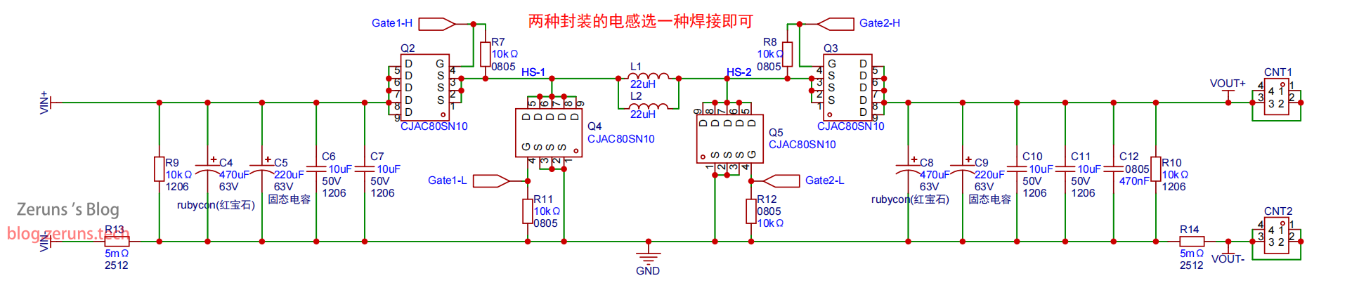
主功率电路整体呈左右对称结构,输入、输出端均各放置470μF/63V铝电解电容与220μF/63V固态铝电解电容各1颗,另加2颗10μF/50V小贴片MLCC,用于端口高频噪声干扰滤波。R9、R10为输入、输出端口假负载,可在断电时快速泄放回路残余能量。R13、R14为5mΩ高精度采样电阻,后级接差分放大电路,对输入、输出电流信号进行放大。CNT1、CNT2为输出端子。L1、L2分别为贴片1770封装与穿孔磁环电感封装,仅需择一焊接,均引出,便于测试不同电感的效果与性能。
电源输入与快充协议电路
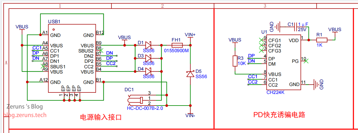
下图为电源输入接口与PD快充协议通信电路图。
电源输入采用DC5.5*2.5mm母座与Type-C母座双接口。Type-C接口支持BC1.2、PD3.0/2.0等多种快充协议,所用快充协议芯片型号为CH224K,可与快充充电器通信,使充电器最高输出20V电压,支持最大功率100W。
二极管D1、D3、D4用于防止DC接口电压反灌至Type-C接口,设计不允许两接口同时接入。D5为反接保护二极管。FH1为电源输入保险丝座,内插12A保险丝。
驱动电路
在同步BUCK-BOOST电源设计中,BUCK与BOOST电路均包含高侧N-MOSFET。传统高侧N-MOSFET驱动通常采用变压器隔离驱动方式,但会增加电路复杂度并扩大板尺寸。
本设计选用两颗内置自举电路功能的MOS管驱动芯片EG3112,分别驱动BUCK与BOOST电路的MOS管。EG3112为非隔离互补双通道驱动芯片,2A输出驱动电流能力确保MOSFET快速导通;芯片内置死区时间控制功能,防止输出驱动信号直通,提高系统稳定性。具体电路如下图所示。
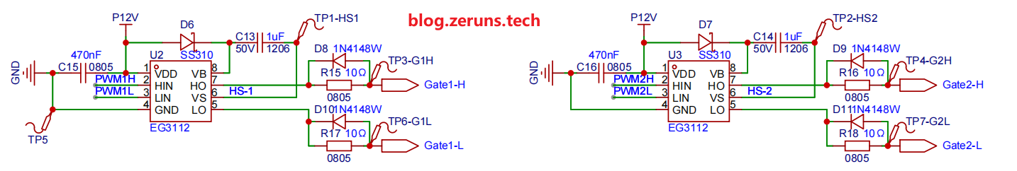
以BOOST升压电路MOS管驱动为例,PWM2L、PWM2H为STM32G474单片机输出的PWM信号,分别送入EG3112驱动芯片的LIN、HIN引脚。LO为下管驱动信号输出,串联10Ω驱动电阻;HO为上管驱动信号输出,同样串联10Ω驱动电阻。D7为上管驱动自举二极管,D9、D11用于快速释放栅极电荷,加快MOS管关断速度,C14为自举电容。
驱动电阻的作用在于MOSFET开关过程中,驱动信号可能在PCB走线、分布电容、电感等元件上产生反射与振荡,串联电阻可抑制此类振荡,提高系统稳定性与可靠性。
辅助电源
下图为电源板辅助电源电路原理图。
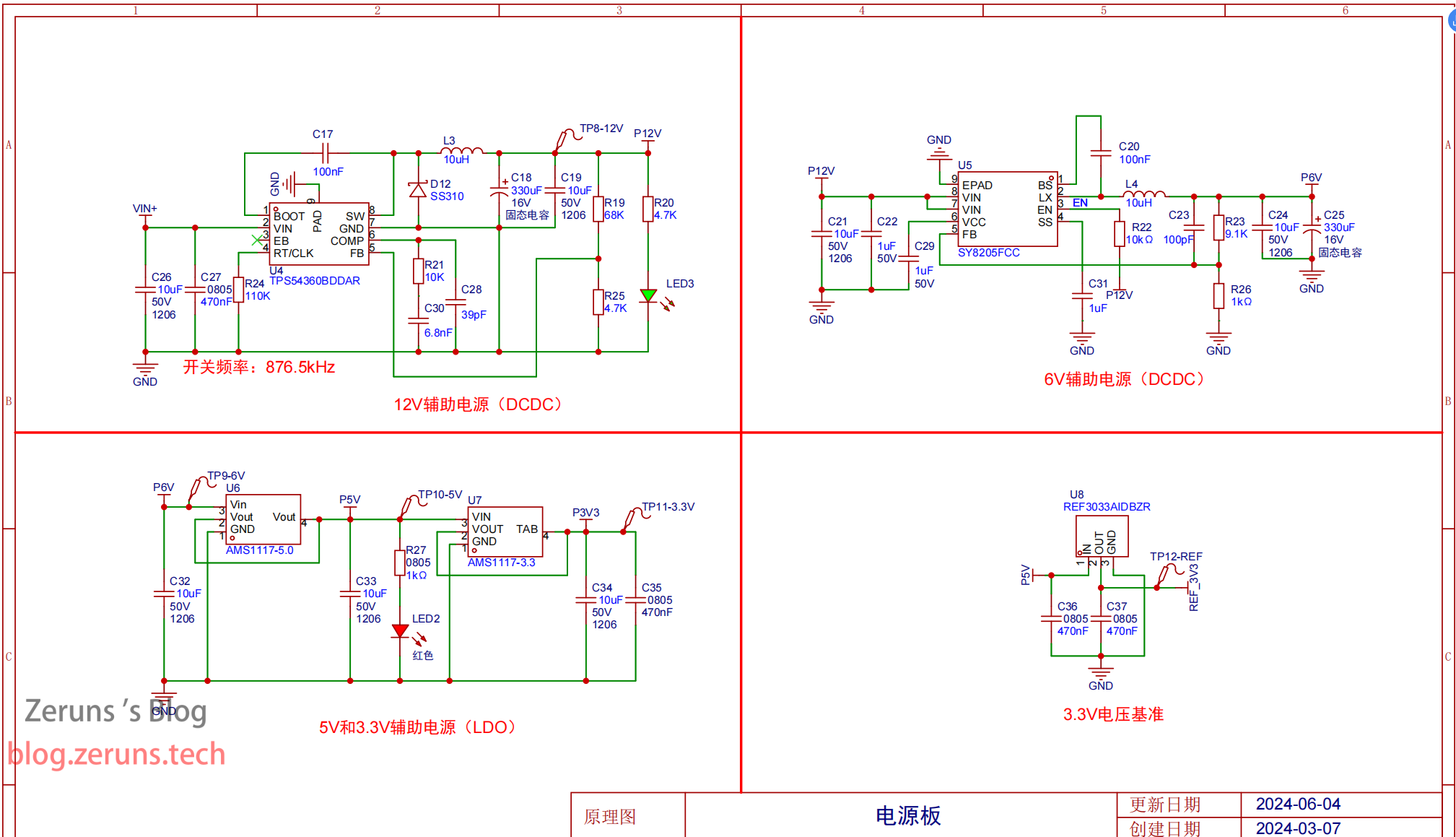
第一级12V输出辅助电源电路采用集成高侧MOSFET的BUCK型电源芯片TPS54360B设计。根据芯片数据手册,RT脚接下拉电阻可设定开关频率,此处选用110kΩ电阻,对应开关频率876.5kHz,较高频率可减小电感体积。按此频率计算,电感值需大于9.75μH,此处选用10μH电感,续流二极管选用SS310。C26、C27为输入滤波电容;反馈分压电阻R19、R25将电压分压后输出0.8V基准电压至芯片FB脚,确保输出电压12V。C18、C19为第一级12V输出辅助电源的滤波电容。第一级12V输出主要用于第二级6V降压电路输入,以及MOSFET驱动电路与散热风扇供电。
第二级6V输出辅助电源电路采用集成MOSFET的同步整流BUCK型电源芯片SY8205设计。根据芯片数据手册,芯片开关频率固定为500kHz,辅助电源BUCK电路电感选用10μH。C21、C22为输入滤波电容;反馈分压电阻R23、R26将电压分压后输出0.6V基准电压至芯片FB脚,确保输出电压6V。C24、C25为第二级6V输出辅助电源的滤波电容。若直接用线性稳压器将12V降至5V,损耗较大,故先用开关电源降至接近5V,再用线性稳压器降至目标电压,可兼顾高效率与低输出纹波。
第二级输出的6V电压经线性稳压器芯片AMS1117-5降压至5V,作为第三级辅助电源,并采用电压基准芯片REF3033,为信号调理、OLED显示、USB通信等功能电路供电。
5V直流电源再经线性稳压器芯片AMS1117-3.3降压至3.3V,作为第四级辅助电源,为MCU、蜂鸣器、Flash芯片等电路供电。电压基准芯片 REF3033 为 MCU 的 VREF 引脚提供 3.3 V 基准电压,作为 MCU 内置 ADC 的参考电压,以提高 ADC 采样精度。
信号调理电路
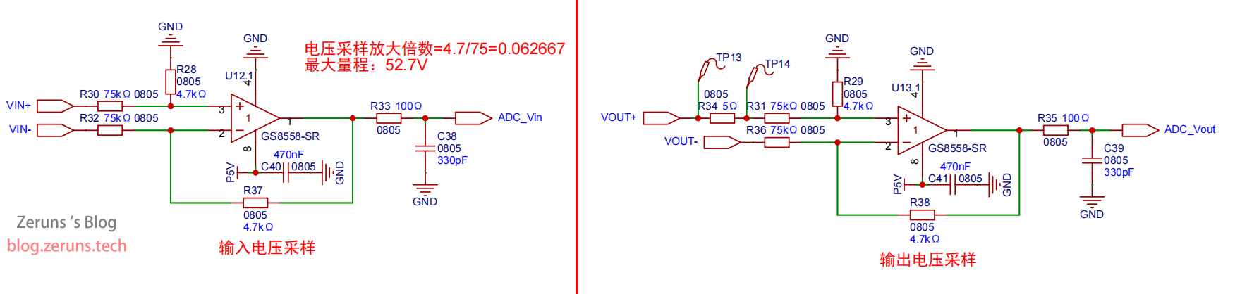
如上图所示,本设计的输入输出电压采样及信号调理电路采用差分放大技术。差分放大拓扑可有效降低开关电源高频噪声对信号调理电路的干扰,提高信号稳定性与可靠性。该电路选用低零漂运算放大器 GS8558-SR,以提升转换精度。GS8558-SR 运放具有出色的直流精度和低偏置电流特性,这对整个信号调理电路的性能提升至关重要。
差分放大电路的反馈电阻:
计算差分放大增益:
MCU 的 ADC 最大采样电压为电压基准芯片输出的 3.3 V,因此可计算最大可采样输入输出电压:
为更好地抑制开关电源高频噪声对差分放大电路的干扰,在运放电源引脚增加去耦电容 C40、C41 进行滤波。电容选用 MLCC(多层陶瓷电容),因其低 ESR 与 ESL,在高频噪声滤波方面效果更佳。同时在输出端增加由电阻 R35 与电容 C39 组成的 RC 低通滤波电路,滤除高频噪声。
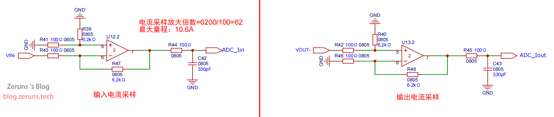
如上图所示,输入输出电流调理电路同样采用差分放大。输出电流采样电阻:
差分放大电路反馈电阻:
计算差分放大增益:
即每 1 A 电流输出 310 mV 电压。
MCU 的 ADC 最大采样电压为电压基准芯片输出的 3.3 V,因此可计算最大可采样输入输出电流:
MCU 控制电路
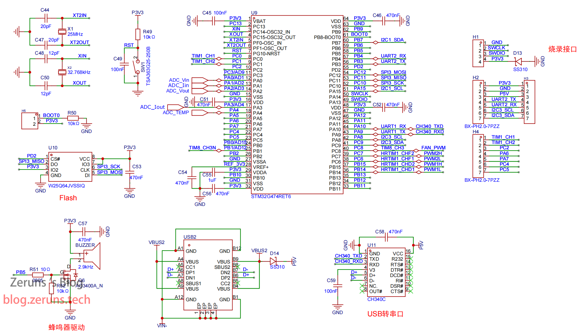
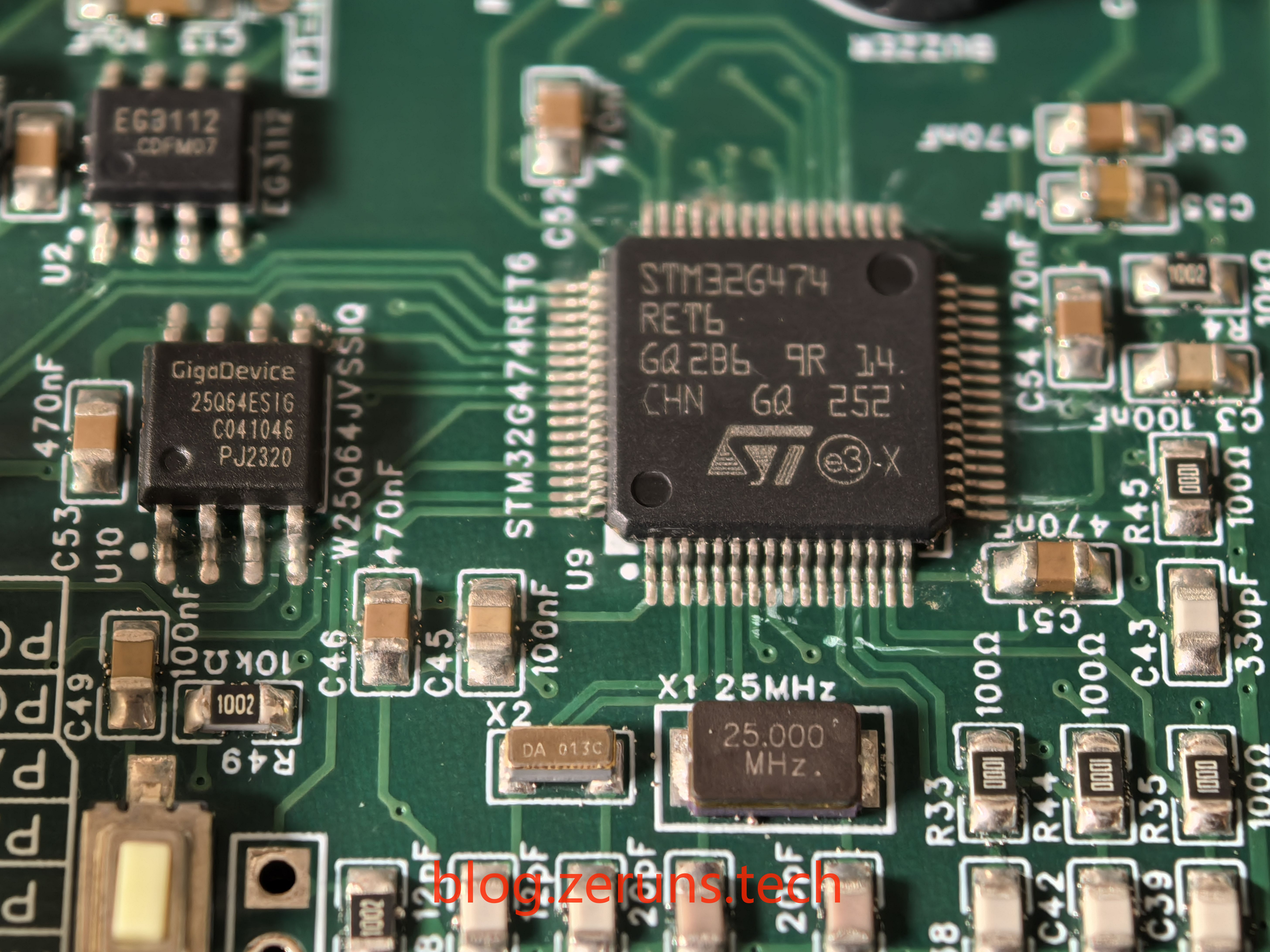
本项目数字电源设计选用 STM32G474RET6 芯片作为控制器,其显著特点是外围电路简单、控制方式多样、扩展能力强。为获得精确时钟信号,控制器采用外部晶振 X1,为 25 MHz 石英晶体。此外,电路包含多个滤波电容:C45、C51、C56、C46、C52,分别用于 MCU 不同数字电源引脚,确保电源稳定并降低噪声干扰。电阻 R49 与电容 C49 构成上电复位电路,SW1 为 MCU 复位按键。U11 为 USB 转串口芯片,型号 CH340C,连接第二路 Type-C 接口,串口连接至 MCU 的 USART1 接口。U10 为 Flash 存储芯片,型号 W25Q64,用于存储参数设置等信息,连接至 MCU 的 SPI3 接口。Q6 为蜂鸣器驱动 MOS 管,用于控制蜂鸣器,MOS 管栅极连接 MCU 的 PB5 口。H1 端子为 SWD 编程口。H2、H4 为 PH2.0 接线端子,用于连接控制面板。端子预留 USART2 接口,可方便地更换为串口屏控制面板方案,也可增加 ESP32 实现联网、无线控制等功能。D13 为 5 V 反接保护二极管。
散热风扇驱动与主板温度采样电路
主板温度采样电路与散热风扇驱动电路原理图如下图所示。电源主板温度采样原理为:NTC 热敏电阻 R2 与下拉电阻 R4 串联分压,输出至 MCU 的 ADC 口采样。所用 NTC 热敏电阻阻值 10 kΩ,B 值 3950 K。
散热风扇采用型号 AO3400 的 N-MOS 管驱动。风扇接口反并二极管 D2,防止电机断电时产生的反电动势损坏器件。电机断电后,由于转动惯性,转子不会立即停止,而是继续旋转并产生电动势,该电动势可能损坏电路中的晶体管或集成电路,特别是当电机通过半导体开关(如 MOSFET)连接时。
![]()
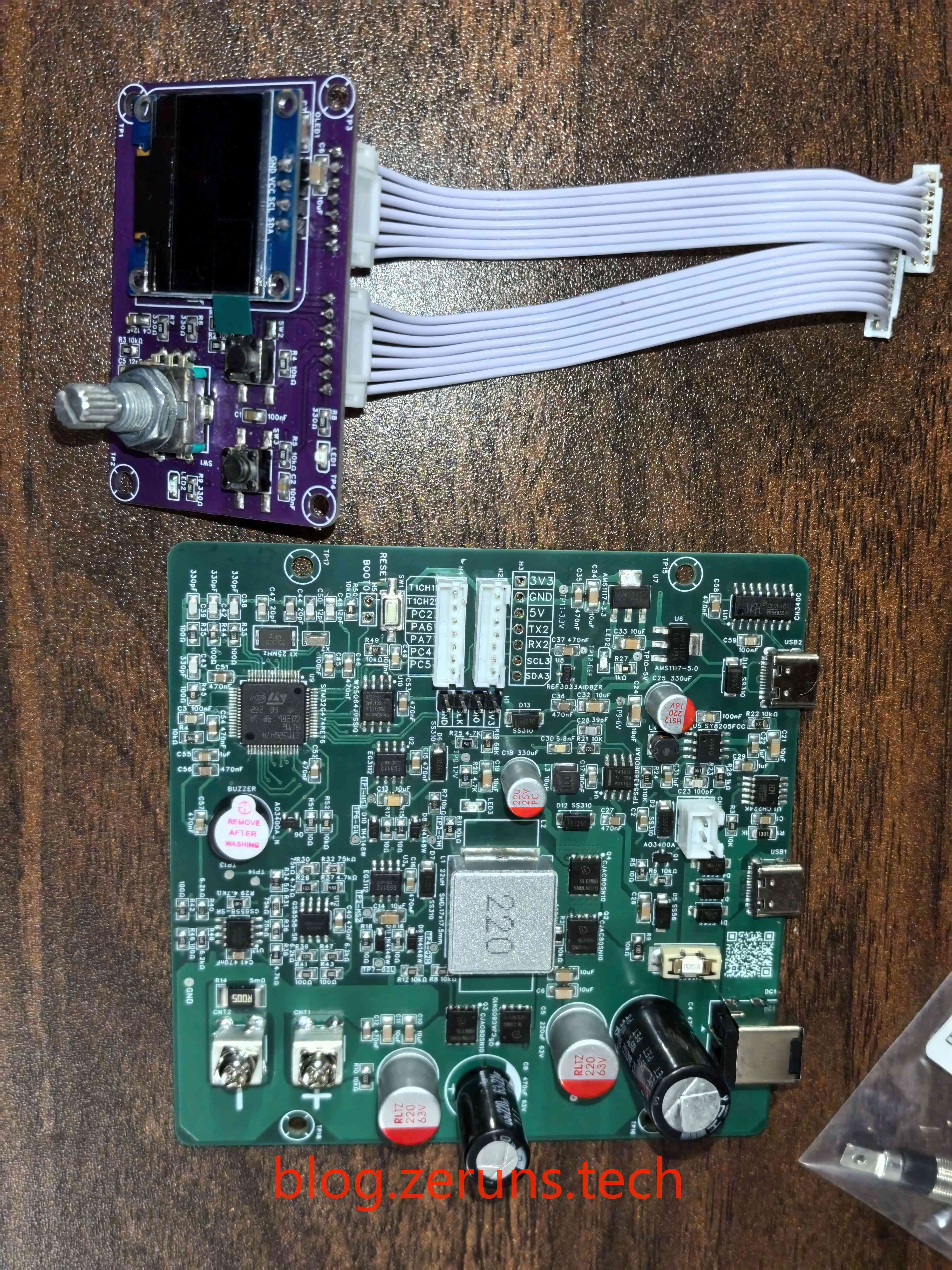
控制面板电路设计
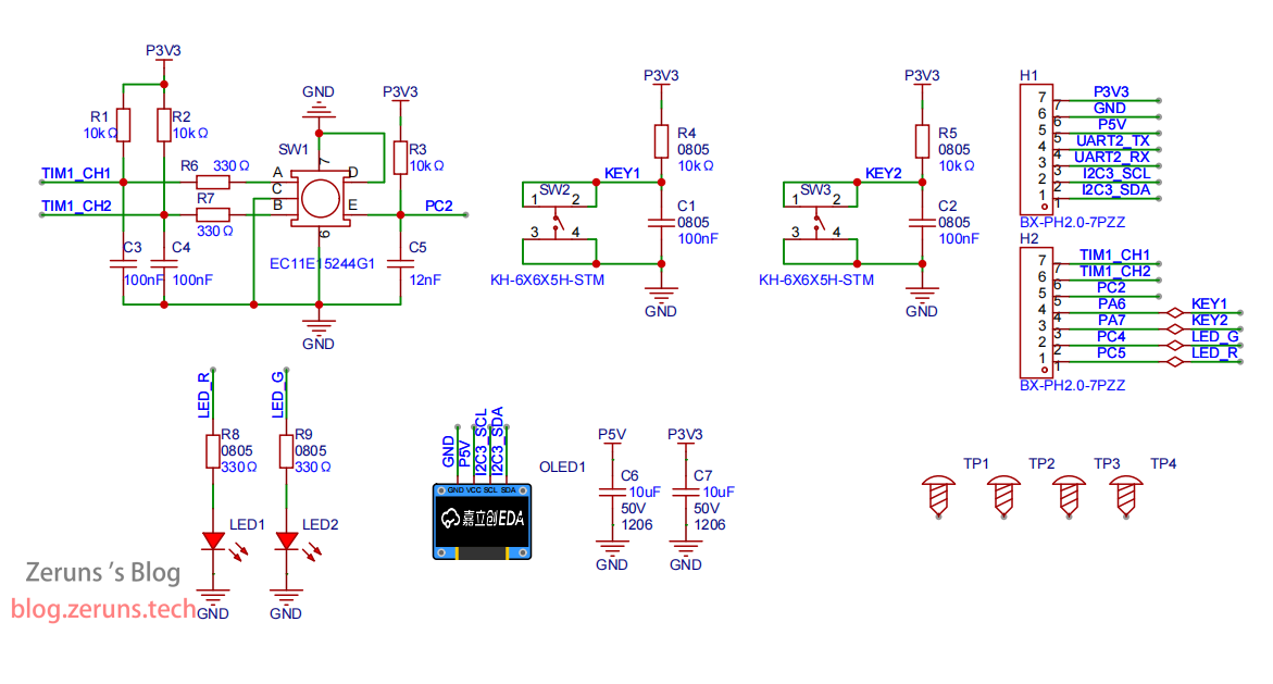
控制面板电路原理图如下图所示。SW1 为旋转编码器,用于参数设置等。SW2、SW3 为按键;SW2 用于切换设置项,SW3 用于控制电源输出开关。LED1 为系统运行状态指示灯,正常工作时以 500 ms 间隔闪烁。LED2 为输出状态指示灯,输出开启时点亮,关闭时熄灭。OLED1 为 OLED 屏,用于显示电源参数与状态。
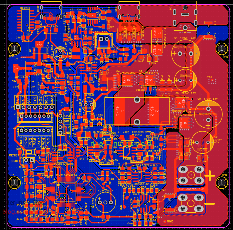
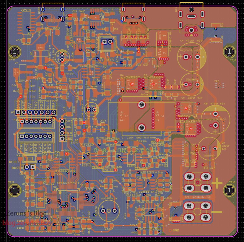
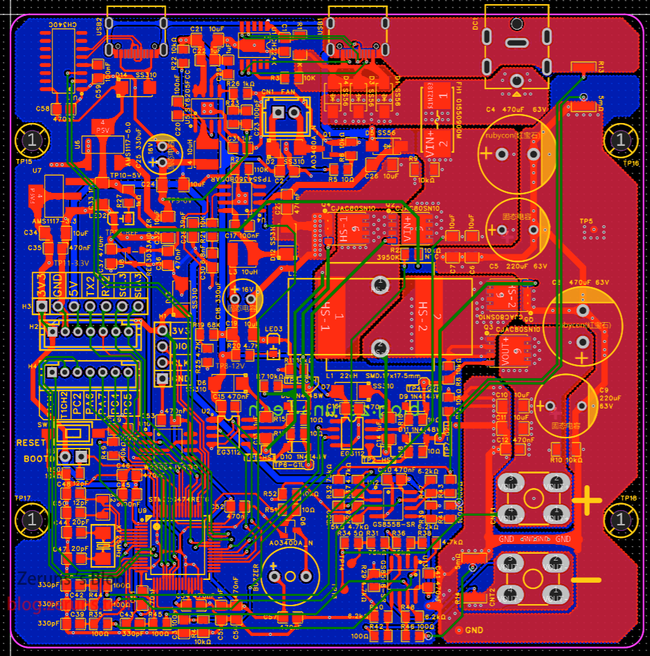
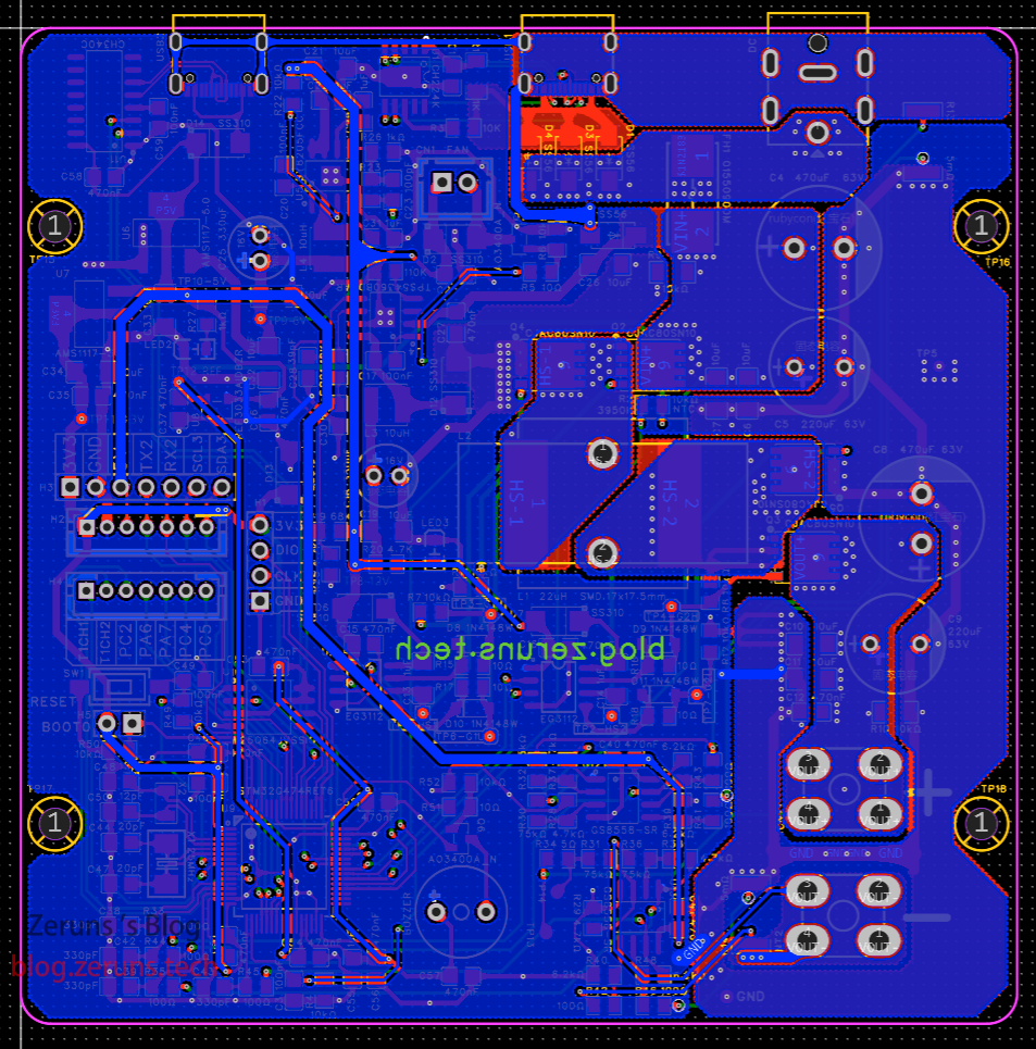
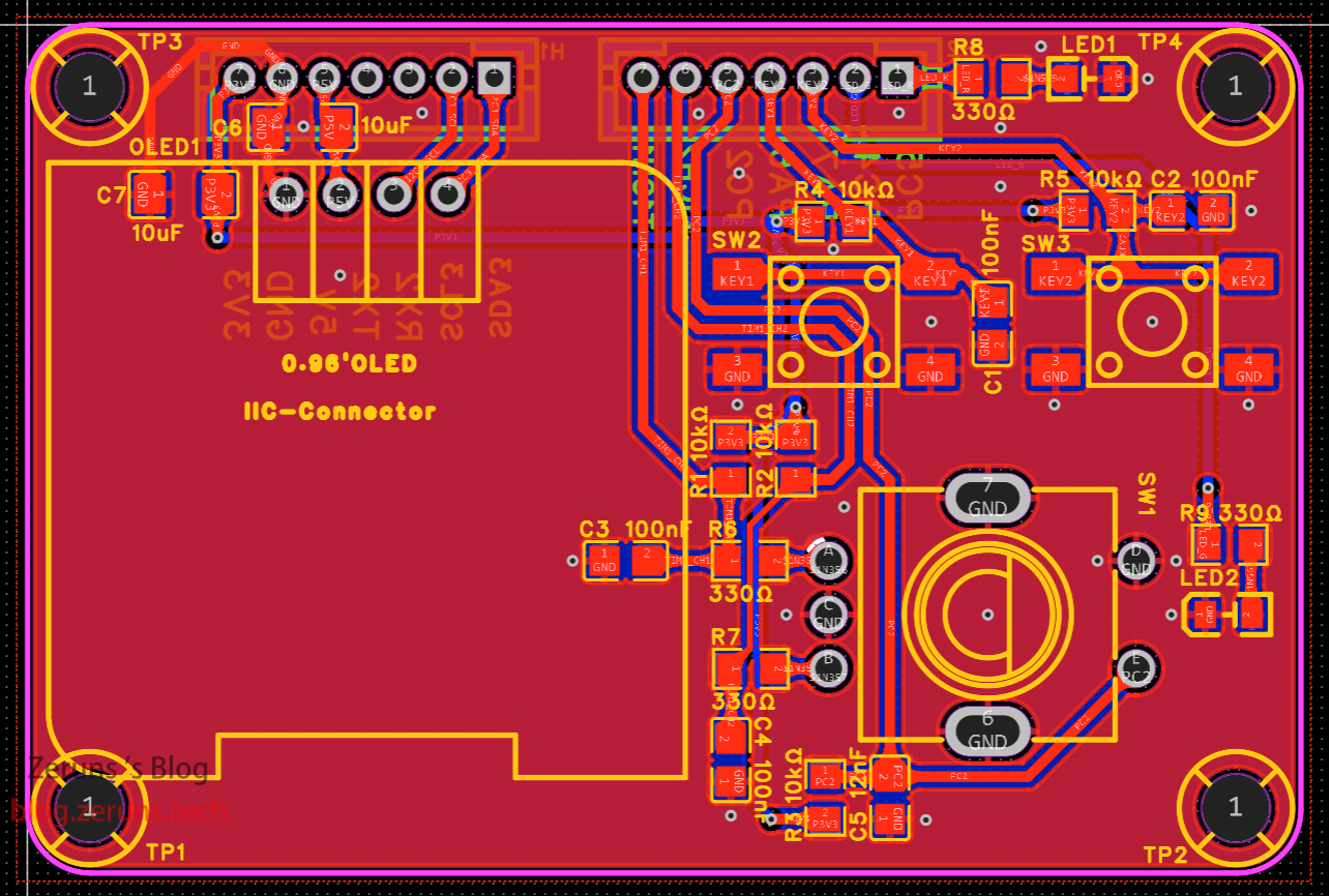
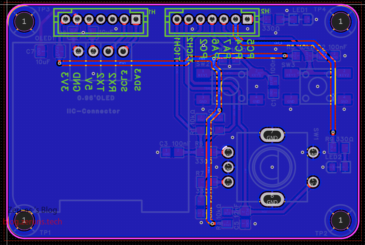
PCB 截图
电源板顶层
电源板 GND 层
电源板内层 2
电源板底层
面板顶层
面板底层
用户手册
可通过按键与旋转编码器设置输出电压、电流值。如下图所示,高亮值为当前待设置位,旋转编码器即可增减数值;按下编码器可切换至下一位设置,通过 SW2 按键可切换待设置项。设置数据将自动保存至 Flash 存储芯片,下次上电时从存储芯片读取。
SW3 按键用于开启/关闭电源输出。
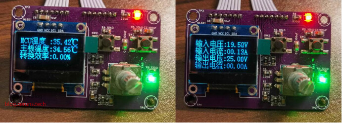
可切换至数据显示页面,查看电源当前输入输出电压、电流,以及主板温度、MCU 温度等信息,如下图所示。
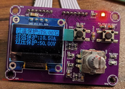
可切换至设置页面,设置过温/过流/过压保护阈值,如下图所示。设置数据将自动保存至 Flash 存储芯片,下次上电时从存储芯片读取。
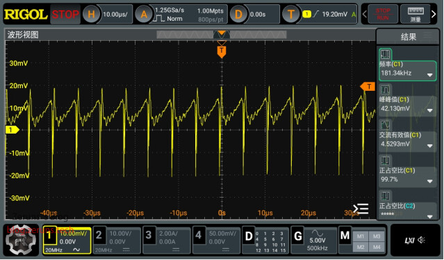
纹波测试
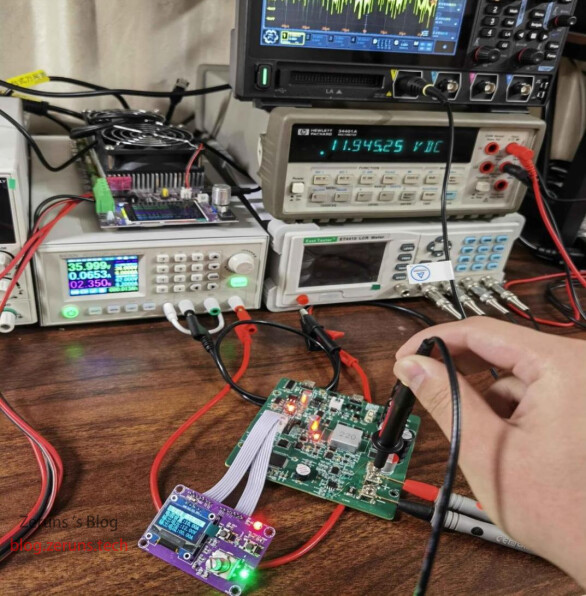
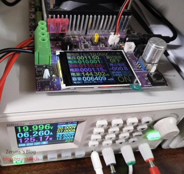
使用电子负载与示波器测试电源输出性能及输出纹波,如下图所示。输入 36 V、输出 12 V/2 A 时,测得峰峰值纹波约 42 mV,如下图所示。
转换效率测试功率转换效率在20V输入和12V10A输出测试时为92%,如下图所示。
下表展示了在不同输入和输出电压下的转换效率,最高效率为94.3%。
| 输入电压 (V) | 输入电流 (A) | 输入功率 (W) | 输出电压 (V) | 输出电流 (A) | 输出功率 (W) | 转换效率 (%) |
|---|---|---|---|---|---|---|
| 20.003 | 4.035 | 80.712 | 15.010 | 5.000 | 75.050 | 92.985 |
| 47.999 | 5.335 | 256.075 | 24.040 | 9.900 | 237.996 | 92.940 |
| 48.000 | 7.875 | 378.000 | 36.020 | 9.900 | 356.598 | 94.338 |
| 48.000 | 9.860 | 473.280 | 45.030 | 9.900 | 445.797 | 94.193 |
| 23.998 | 8.835 | 212.022 | 48.070 | 4.000 | 192.280 | 90.689 |
| 23.998 | 9.830 | 235.900 | 35.998 | 6.001 | 216.024 | 91.574 |
| 12.099 | 9.166 | 110.899 | 24.070 | 4.000 | 96.280 | 86.817 |
| 20.008 | 2.645 | 52.921 | 4.970 | 9.000 | 44.730 | 84.522 |
| 20.008 | 10.550 | 211.084 | 24.030 | 8.000 | 192.240 | 91.073 |
| 36.000 | 6.418 | 231.048 | 24.010 | 9.000 | 216.090 | 93.526 |
| 36.000 | 10.540 | 379.440 | 35.950 | 9.800 | 352.310 | 92.850 |
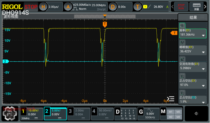
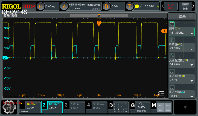
MOSFET栅极波形
在输入20V、输出24V时测试各MOS的栅极波形。
BUCK电路上下管相对于地的电压波形:
BOOST电路上下管相对于地的电压波形:
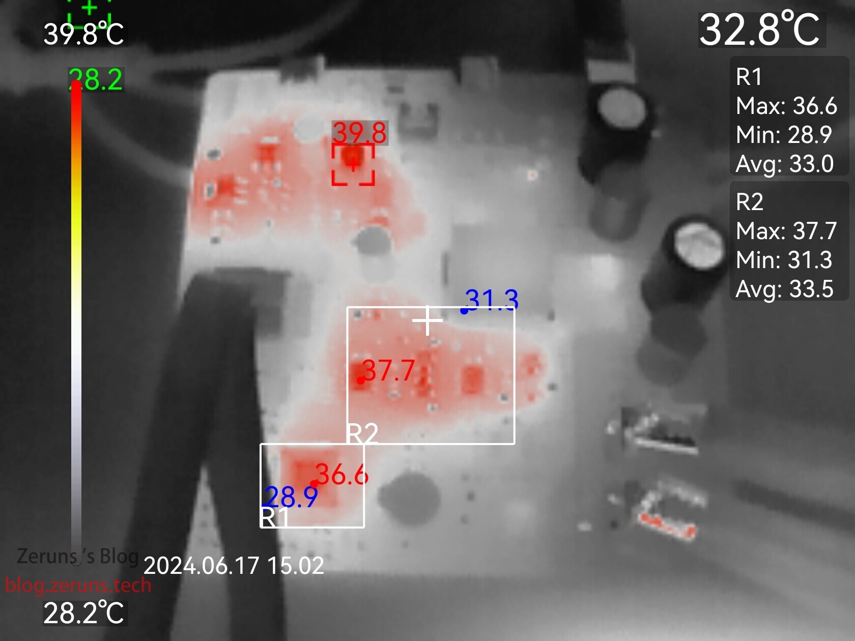
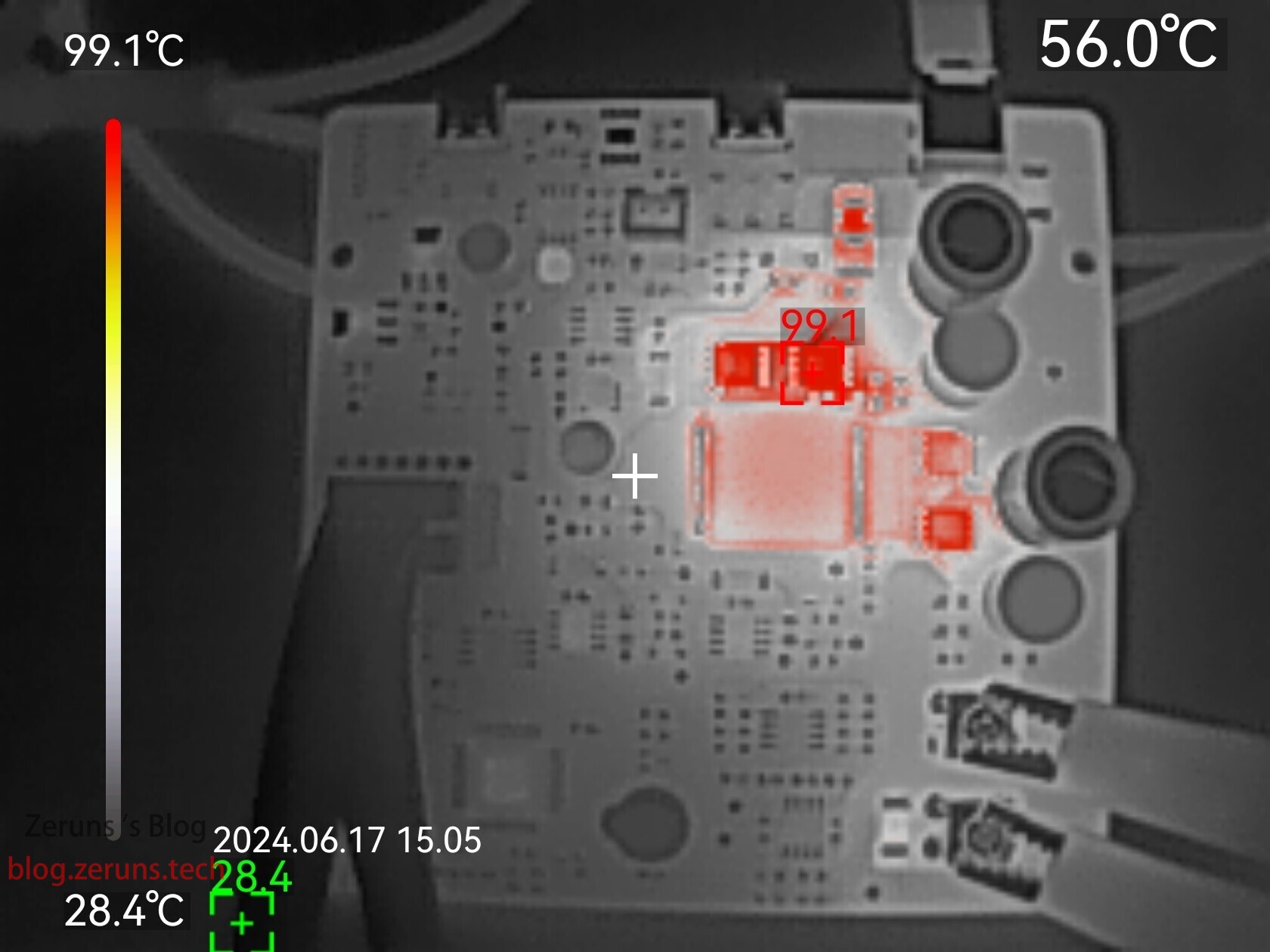
发热测试
空载条件下的热成像图:
输出10A电流10分钟后的热成像图,MOS管温度约为100度:
优利德UTi261M热成像仪开箱评测:https://blog.zeruns.com/archives/798.html
元器件购买链接
本项目使用的大部分元器件购买链接如下:- 0805 电阻和电容样品册:https://s.click.taobao.com/begdskt
- STM32G474RE 芯片:https://s.click.taobao.com/C5yYWlt
- CH224K 芯片:https://s.click.taobao.com/4t4bskt
- CJAC80SN10 MOSFET:https://s.click.taobao.com/aPsWWlt
- EG3112 芯片:https://s.click.taobao.com/1k9Zskt
- 220μF 63V 固态电容:https://s.click.taobao.com/n60Yskt
- 470μF 63V Rubycon 电容:https://s.click.taobao.com/WTRUWlt
- GS8558 运算放大器:https://s.click.taobao.com/usSVskt
- TPS54360 芯片:https://s.click.taobao.com/r6lSWlt
- SY8205 芯片:https://s.click.taobao.com/GxMUskt- AMS1117芯片:https://s.click.taobao.com/mxASWlt
- REF3033基准芯片:https://s.click.taobao.com/eOcTskt
- W25Q64JVSSIQ芯片:https://s.click.taobao.com/QX7Tskt
- CH340C芯片:https://s.click.taobao.com/QYRQWlt
- 3.3V有源蜂鸣器:https://s.click.taobao.com/sovPWlt
- TypeC母座16P:https://s.click.taobao.com/vjLRskt
建议在LCSC商城购买元器件:https://activity.szlcsc.com/invite/D03E5B9CEAAE70A4.html
点击LCSC开源链接BOM列表中的“立即在LCSC商城购买”即可一键导入所需元器件到购物车。
资料下载链接
以下链接包含LCSC EDA工程、原理图PDF文件、各芯片数据手册、源码工程压缩包、部分参考程序代码等资料。
123Pan不限速下载链接: https://www.123pan.com/ps/2Y9Djv-8yevH.html
百度网盘下载链接:https://url.zeruns.com/MW2d1
项目程序Gitee开源链接: https://gitee.com/zeruns/STM32-Buck-Boost
项目程序GitHub开源链接:https://github.com/zeruns/Synchronous-Rectification-Buck-Boost-Digital-Power-Supply-Based-on-STM32
请给个Star和点赞。
已知问题
- 辅助电源的SY8205芯片在轻载时会进入PFM模式,频率较低,会有轻微响声。
- 恒流模式的PID控制程序写得不好,恒流仅在纯阻性负载下稳定。(恒压模式无问题)
推荐其他开源项目
- 自制了一个三相电量采集器并开源,可方便监测家庭用电情况:https://blog.zeruns.com/archives/771.html
- STM32F407的LVGL项目模板(MSP3526屏幕),含FreeRTOS版本和裸机版本:https://blog.zeruns.com/archives/788.html
- 沁恒CH32V307VCT6最小系统板开源:https://blog.zeruns.com/archives/726.html
- LM25118自动升降压可调DCDC电源模块:https://blog.zeruns.com/archives/727.html
- EG1164大功率同步整流升压模块开源,最高效率97%:https://blog.zeruns.com/archives/730.html
- 基于合宙Air700E的4G环境监测节点(温湿度、气压等数据),通过MQTT上传至阿里云物联网平台:https://blog.zeruns.com/archives/747.html
- 基于HT32F52352的智能电子负载开源,合泰杯参赛作品:https://blog.zeruns.com/archives/784.html
推荐阅读- 性价比高的便宜VPS/云服务器推荐: https://blog.zeruns.com/archives/383.html
- Minecraft 服务器搭建教程:https://blog.zeruns.com/tag/mc/
- 零基础搭建博客网站!超详细个人博客搭建教程:https://blog.zeruns.com/archives/783.html
- 内网穿透服务器搭建教程,NPS 搭建和使用教程:https://blog.zeruns.com/archives/741.html
- 雨云宁波 8272CL 大带宽高防云服务器性能评测,最高 500Mbps 带宽和 1TB 云盘:https://blog.zeruns.com/archives/789.html
- 抖音商城 2.6 元 120W 充电器测试拆解:https://blog.zeruns.com/archives/786.html