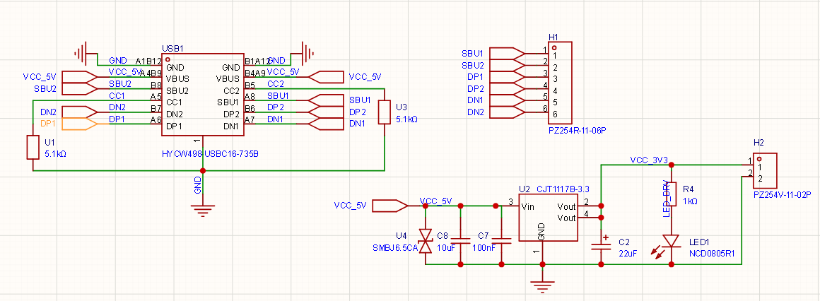
Use a 16-pin Type-C connector as the input port, retaining signal lines (other than power lines) and routing them out via pin headers for future use.
Power lines go through TVS electrostatic protection and capacitor filtering before connecting to the input of the 1117 regulator.
After the 1117 output, use a 22μF tantalum capacitor for filtering, and connect an LED in parallel as a power indicator.
Route the output power to pin headers for easy access.
Questions & Concerns
The Type-C wiring looks messy—is this schematic drawing practice actually up to standard?
When using pin headers to route out the six Type-C signal lines, does the order matter? I just arranged them randomly.
Is my TVS diode selection appropriate? Does it meet the circuit requirements?
Can the tantalum capacitor be replaced with an alternative solution? Would MLCC + small resistor or MLCC + aluminum electrolytic capacitor be better options?
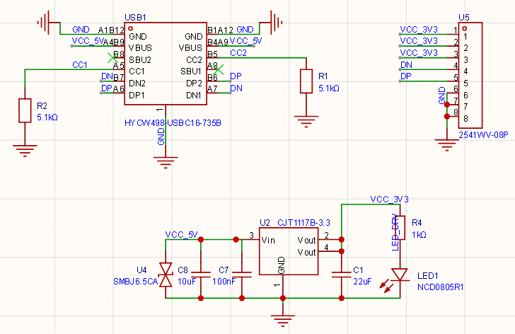
The DP1, DP2 and DN1, DN2 pins of the Type-C interface should be shorted together respectively, because Type-C supports plug-and-play in both orientations—therefore, both upper and lower contacts have a pair of DP and DN. Shorting them ensures functionality regardless of plug orientation. Additionally, when routing on the PCB, DP and DN should be routed differentially.
Using net labels is sufficient; there’s no need to add extra input/output symbols.
The pinout order of the header can be arranged according to your own requirements; there are no strict rules.
The TVS selection is appropriate and presents no issues.
The LDO output filter can directly use MLCC capacitors (although some older versions of the 1117 may experience internal loop instability causing output oscillation when using MLCC, newer domestic versions of the 1117 generally do not have this issue).
Rare to see such a detailed and well-structured question—clear thinking, with diagrams, and precisely articulated points of confusion. This is what a standard good question should look like!
The worst are those who can’t even clearly describe their own problem, and you have to keep asking them questions just to figure out what they’re actually asking
Hello! As a beginner, your schematic diagram is excellent! The overall logic is clear: the Type-C CC pin pull-down resistors (5.1kΩ each for U1 and U3) are correctly implemented, input and output capacitors for the LDO are fully provided, and you’ve even considered TVS protection—this already surpasses many beginners.
Now, let me address your questions one by one and provide some practical engineering suggestions:
1. Are the messy Type-C wiring lines acceptable in schematic drawing standards?
Your current wiring is electrically correct, but from the perspective of schematic “readability” and “aesthetics,” there’s room for improvement.
Improvement Suggestion: In real engineering practice, to avoid visual clutter caused by crossed wires, we usually use net labels. You can extend a short segment from the USB connector pins and assign them net labels (e.g., name them DP1, DN1), then do the same on header H1 with matching net labels. The software will automatically connect these nets, making your schematic much cleaner.
2. Signal pin order on the header
From a purely conductive standpoint, any pin order would work. However, considering signal integrity and future usability, follow these principles:
Critical Omission: Missing GND! Your header H1 has only signal lines and no ground. Every signal needs a return path. Without an explicit GND connection, when you use jumper wires to connect these signals to another board, differences in ground potential may cause communication failure or even damage devices. Be sure to add at least one GND pin to H1.
Signal Merging and Ordering: For standard USB 2.0 communication, a Type-C receptacle internally has two pairs of D+/D- to support reversible insertion. Typically, near the connector, we short DP1 with DP2 and DN1 with DN2. This way, you only need to route out one pair of D+ and D-.
Recommended Pin Order: GND, SBU1, SBU2, DP, DN. Place the differential pair (DP and DN) adjacent to each other for easier wiring later.
3. Is the TVS selection (SMBJ6.5CA) appropriate?
The choice is very safe and meets requirements well—though slight optimization is possible.
Parameter Analysis: The normal operating voltage of USB VBUS is 5V. The reverse standoff voltage (Vrwm) of SMBJ6.5CA is 6.5V, which prevents leakage during normal 5V operation while effectively clamping overvoltage spikes—a precise parameter match.
Optimization Suggestions:
The suffix CA indicates a bidirectional TVS. For DC power lines (VCC_5V), it’s actually better to use a unidirectional TVS (suffix A, e.g., SMBJ6.5A), as unidirectional TVS diodes offer superior clamping for negative voltage transients.
Package size: The SMB package is somewhat large for a simple LDO step-down board. If compactness is desired, consider switching to SMAJ6.5A (SMA package) or even smaller ESD protection devices in SOD-323 packages. Of course, if you already have SMBJ6.5CA on hand, using it is perfectly fine.
4. Alternatives to Tantalum Capacitors (“Pitfall” of the 1117 chip)
You’ve touched on a very professional and critical point! The 1117 series regulators have strict requirements regarding the ESR (Equivalent Series Resistance) of the output capacitor.
The 1117 uses an older bipolar LDO architecture that relies on the output capacitor having a certain amount of ESR (typically required between 0.1Ω and 10Ω) to maintain internal loop stability.
Using only MLCCs (ceramic capacitors): MLCCs have extremely low ESR (often just a few milliohms), which can cause the 1117 to oscillate, resulting in high-frequency ripple on the output instead of a clean, stable 3.3V DC.
Recommended Alternatives:
Option A (Most Recommended, Best Cost-Performance): 100nF MLCC in parallel with a 10μF (or 22μF) aluminum electrolytic capacitor. Aluminum electrolytics naturally have adequate ESR, satisfying the 1117’s anti-oscillation requirement; the added 100nF MLCC filters high-frequency noise. This is the most common and cost-effective solution in engineering practice.
Option B (Compact Size): 22μF MLCC in series with a small resistor (e.g., 0.5Ω or 1Ω). Use the resistor to artificially create ESR. While feasible, this adds component complexity and is less elegant than Option A.
Summary: Using tantalum capacitors as you currently are works perfectly fine (tantalum caps have just the right ESR), but they are expensive and prone to catching fire under overvoltage. We recommend replacing them with the MLCC + aluminum electrolytic capacitor combination.
One Final Small Tip:
Current-limiting resistor R4 (1kΩ) for the LED indicator: (3.3V - LED forward voltage ~2V) / 1kΩ ≈ 1.3mA. This current might make a standard SMD LED appear slightly dim. If you’d like it brighter, consider changing R4 to 470Ω or 510Ω (resulting in ~2.5mA–3mA current).
This is a very solid first attempt at an LDO buck circuit! You’ve successfully grasped the core concepts: negotiating 5V from a Type-C port using CC resistors, adding input protection, filtering, and providing an output indicator. Electrically, this circuit will successfully output 3.3V.
Here is a breakdown of your questions and some expert tips to level up your schematic design.
1. Schematic Drawing & Type-C Wiring Standard
Your schematic is absolutely readable, but there are a few standard conventions you can apply to make it cleaner and more professional:
Component Designators: You used U1 and U3 for your 5.1kΩ CC resistors. In schematic standards, U is reserved for Integrated Circuits (like your 1117 and TVS). Resistors should always use R (e.g., R1, R2).
Net Labels vs. Wires: While drawing explicit green wires is fine for a simple circuit, crossing them over each other (like your DP/DN and SBU lines) can get messy. In professional design, we use Net Labels (naming a stub of a wire “DP1” and naming the receiving end “DP1”) to invisibly connect them without drawing a line across the page.
Visual Flow: Standard practice is to have inputs on the left, the main processing/power conversion in the middle, and outputs on the right. You’ve mostly followed this, which is great!
2. Signal Header (H1) Pin Order
If you are just breaking these out to a header for jumper wires, the physical order doesn’t strictly matter. However, if you plan to use this for data, there are best practices:
Group Differential Pairs: USB 2.0 relies on differential pairs (DP and DN). They should be placed right next to each other. A better order would be: DP1, DN1, DP2, DN2, SBU1, SBU2.
The USB 2.0 Flip “Gotcha”: Type-C is reversible. If you plug a cable in right-side up, data travels on DP1/DN1. If you flip it upside down, data travels on DP2/DN2. If you want to use this for a USB 2.0 data connection later regardless of cable orientation, you should short DP1 to DP2 and DN1 to DN2 right at the connector, and route just one pair (DP/DN) to your header.
3. TVS Diode Selection (SMBJ6.5CA)
Your choice of the SMBJ6.5CA is safe and will work, but it can be slightly optimized.
Voltage Rating: The “6.5” means a standoff voltage of 6.5V. This is perfect for a 5V USB line, as it won’t accidentally trigger during normal operation, but will clamp voltage spikes before they hit the 15V absolute maximum rating of the 1117.
Directionality (CA vs A): The “CA” suffix means it is Bidirectional. Because your USB VBUS is a strictly positive DC supply, a Unidirectional TVS (SMBJ6.5A) is actually preferred. A unidirectional TVS provides better protection against negative voltage transients (clamping them at a harmless -0.7V), whereas a bidirectional one would allow a negative spike to reach roughly -11V before clamping.
4. Output Capacitor & The “1117 ESR Trap”
You’ve stumbled upon the most famous quirk in PCB design: the 1117 LDO stability requirement.
Older LDO architectures like the 1117 require their output capacitor to have a specific amount of Equivalent Series Resistance (ESR)—usually between 0.3Ω and 22Ω—to maintain control loop stability.
Your current choice (Tantalum): Tantalum capacitors naturally fall right into this required ESR range. This is why tantalums are the classic, correct pairing for an 1117.
Alternative 1: MLCC + Small Resistor: Yes, this is an excellent and common alternative! Pure ceramic capacitors (MLCCs) have virtually zero ESR, which causes the 1117 to oscillate and output a noisy, unstable voltage. If you want to use a cheap 10μF or 22μF MLCC, placing a 0.5Ω to 1Ω resistor in series with it perfectly mimics a tantalum cap.
Alternative 2: MLCC + Aluminum Electrolytic: This also works. The electrolytic provides the necessary ESR, while the MLCC handles high-frequency noise.
Pro Tip: If you want to avoid the headache of ESR entirely, simply swap the 1117 for a modern “ceramic-stable” LDO (like the AP2112 or RT9013). They are designed to work perfectly with standard MLCCs without any extra resistors.
It’s only like this with the Type-C interface because Type-C allows insertion in either orientation, and the upper and lower contacts are the same pins, so they need to be connected together when brought out.
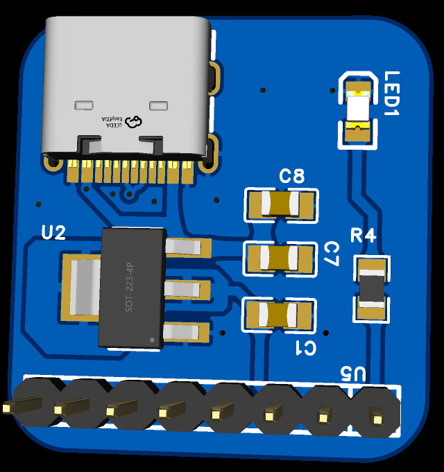
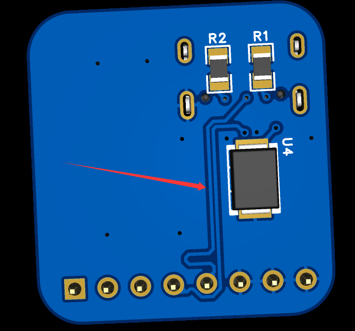
I adjusted the schematic according to your suggestions. I’m not sure if I understood your second point correctly—could you please help me check it? Also, I’ve drawn the PCB, but I feel the differential pairs might not be done quite right.
The TVS should be placed close to the interface, and the trace must go through the TVS before connecting to other components; otherwise, it won’t function properly.
It’s better to add ESD protection diodes on the DP and DN data lines as well, although most modern chips already have built-in ESD protection.
USB signal traces require 90Ω impedance matching and length tuning (though for low-speed signals, this is not strictly necessary).
You can explore more designs from others on LCSC’s Open Source Platform to learn and improve.
Power networks can be directly connected using custom copper pours.
The TVS could be replaced with a smaller package version.
I’ve thought about it… those two differential pairs, if they need to be shorted, would require either via holes or routing around in a large loop… or alternatively, just route the two differential pairs so that they naturally connect at the output end.
It’s not recommended to do this, as it will cause signal integrity issues. Below is the AI analysis for your reference:
This approach is strongly discouraged in circuit design and typically leads to severely degraded signal quality, or may even result in device recognition failure or frequent disconnections.
A simple and direct conclusion: Do not route two differential pairs to a remote point and then merge them. Instead, merging should be done locally near the Type-C connector pads, followed by routing as a single differential pair.
Here are the key problems caused by this “dual-pair routing” method:
1. Critical “Stub Effect”
USB Type-C supports reversible plug insertion, but at any given time, data travels through only one DP/DN pair (depending on plug orientation).
If you route two differential pairs and merge them remotely, when the cable is plugged in, one pair carries the signal while the other becomes an open-ended “stub”.
Under high-frequency signals (USB 2.0 operates at 480 Mbps with very fast rising edges), this floating trace causes severe signal reflections. The reflected signals interfere with the original signal, leading to eye diagram closure and a sharp increase in bit error rate.
2. Impedance Discontinuity
Differential traces require strict impedance control (typically 90\\Omega \\pm 10\\%).
At the junction where the two pairs meet (a “T-junction”), the impedance changes drastically—momentarily halved due to parallel connection.
Such impedance discontinuities are sources of signal reflection, degrading signal integrity.
3. EMI (Electromagnetic Interference) Issues
The idle trace pair not only causes reflections but also acts like an antenna, radiating high-frequency noise outward or picking up surrounding electromagnetic interference. This makes it difficult for your product to pass EMC certification.
Recommended Best Practice Solutions
To ensure good signal quality, use one of the following two approaches:
Solution A: Direct Merging at Pads (Most Recommended)
On the top or bottom PCB layer, directly connect A6 to B6 and A7 to B7.
Implementation: Use “inside-cut” or “cross-over” routing to quickly merge the two pad groups.
Advantages: Minimal stub length, best impedance continuity, and saves routing space.
Solution B: Inner Layer Merging
If board space is extremely limited, place vias under both pad groups and merge them via the inner layer using the shortest possible path.
Note: The distance from the via to the pad should be as short as possible (ideally less than 50 mil).
Comparison Aspect
Remote Merging
Near-end Merging (Recommended)
Signal Integrity
Poor (severe reflections)
Excellent
Eye Diagram Quality
Noisy, prone to closure
Clean, wide opening
Routing Difficulty
High (requires maintaining two differential pairs)
Low (only one differential pair)
Certification Risk
Very high (difficult to pass USB-IF)
Low
Additional Recommendations
If you’re using a 16-pin connector, it’s usually intended for charging or USB 2.0 communication. Please ensure:
Matched Lengths for Differential Pairs: Keep the length difference between DP and DN within 5 mil.
Avoid Noise Sources: Route differential traces away from power modules (DC-DC converters) and clock signals.
Solid Ground Plane: Maintain an unbroken reference ground plane beneath the traces; avoid crossing split planes.
Awesome!! I couldn’t find a reference image for the longest time, but as soon as I saw the picture, everything became clear. Thank you so much,大佬, for the help!!!