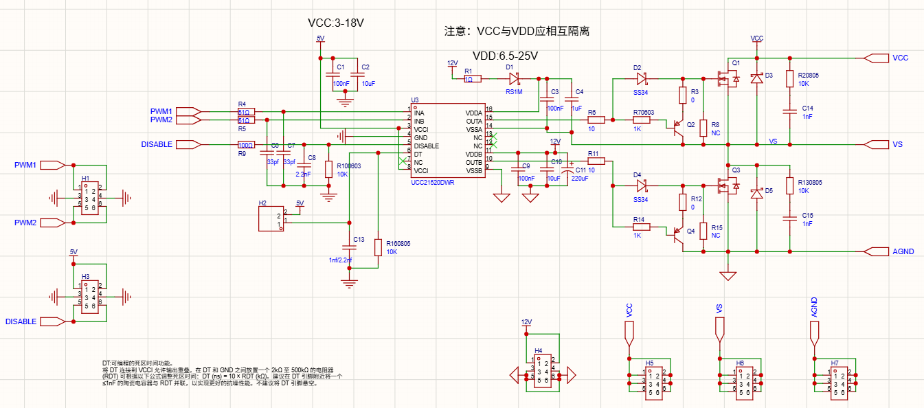
The schematic is shown above. I connected 5 V to the VS port in series with a 470 µH inductor (low-voltage side), then connected a 1000 µF capacitor and a 1 kΩ resistor in parallel at the VCC terminal. PWMA and PWMB are fed PWM signals with dead time from the microcontroller (currently just 50% duty cycle, with no feedback). Now the output voltage at VCC is only about 4.6 V (I suspect it’s just the Schottky diode voltage drop), and PWMA and PWMB still show this output even when there is no signal. Could the experts here please suggest some directions for fixing this? ![]()
At the moment, it seems that neither the upper nor lower tube has a conduction signal, so only the Schottky diode connected in parallel with the upper tube of the DC current path is present.
Have you connected 12V? The UCC21520 is an isolated driver, and both channels’ outputs need to be connected to independent power supplies.
Here’s another post about UCC21520 issues: https://bbs.eeclub.top/t/topic/284/2
Bro, this is 100% a case where the upper tube isn’t switching at all. The current is going straight through the upper tube’s body diode — or the Schottky diode you added in parallel — for freewheeling. Your input is 5V, and after subtracting the diode drop, you end up right around the 4.6V you measured.
I’d suggest checking these steps:
-
Is the 12V auxiliary supply connected? From your schematic, VDDB needs an independent 12V supply. If that 12V isn’t there, the driver chip will be in UVLO (undervoltage lockout), and no matter how much PWM signal the MCU sends, the chip will just ignore it.
-
DISABLE pin state: Even though the schematic has R10 (10k) pulling it down, it’s best to measure pin 5 of the UCC21520 with a multimeter and make sure it’s really at 0V. If it’s floating or being pulled high by noise, the chip won’t output anything.
-
Check the lower tube first: The Boost converter relies entirely on the lower tube (Q3) turning on to store energy in the inductor. If the lower tube isn’t conducting, everything else is pointless. Don’t worry about the upper tube for now — take the oscilloscope and measure the G terminal of Q3 directly, and see whether you have a square wave.
Without even an oscilloscope waveform to look at, how am I supposed to diagnose it… I’ll take a blind guess at a few common pitfalls:
First, grounding issues. Your PWM signal comes from the microcontroller—have you connected the microcontroller’s GND to the ground on the driver chip’s input side (pin 4, GND)? If the grounds on the two sides of the optocoupler or isolation chip aren’t handled properly, the signal simply won’t get through. Second, a bootstrap circuit deadlock. When using a half-bridge driver for a Boost converter, the bootstrap capacitors for the high-side switch (C3 and C4) charge when the low-side switch turns on and pulls VS to ground. If, for some reason, the low-side switch doesn’t turn on (for example, the driver-side VDD has no power, or the fast-shutdown circuit is soldered backward), then the high-side VDDA will never charge, and the high-side switch will never turn on either.
The troubleshooting approach is simple: disconnect the main circuit’s 5 V input, power only the control board and driver board, then use your probe to check pin 11 (OUTB) on the chip. You must first see a 50% duty-cycle square wave there before going any further.
Hey man, classic gate driver issue! If your output is sitting at 4.6V even when you apply no PWM, it means the circuit is just acting as a passive wire and the low-side FET isn’t doing its job to charge the inductor.
A couple of quick things to check on your board:
-
UVLO (Under Voltage Lockout): Did you actually provide the 12V to the VDDB pin? The UCC21520 will completely ignore your MCU signals if the secondary-side supply voltage is missing or below the threshold.
-
DISABLE pin: Measure pin 5 on the IC directly with a multimeter. Even though you have R10 doing a pull-down, make sure it is solidly at 0V.
-
Logic Levels: Is your MCU outputting 3.3V or 5V logic? Ensure it meets the V_IH (input high threshold) of the driver.
Grab a scope and check the OUTB pin (pin 11). Don’t even worry about the high side or the 5V main power until you see a clean, crisp square wave on the low-side gate!
The lower tube won’t open. Right now, when the microcontroller isn’t connected, I can measure a PWM waveform at the output, but once I connect PWMA and PWMB, the PWM waveform disappears and turns into a few hundred millivolts of noise
What waveform do you want to see, bro?
The lower tube won’t turn on. When the MCU isn’t connected, I can measure a PWM signal at the output, but as soon as I connect PWMA and PWMB, the PWM signal disappears and turns into a few hundred millivolts of noise ![]()
Bro, I haven’t worked with an isolated power supply before. Does “isolated power supply” mean the grounds are connected separately to two different ground points? Can I put a resistor between AGND and GND?
What does the measured output waveform look like? Send a picture!
Also measure the PWM waveform output by the microcontroller and send a picture!
Measure both the input and output waveforms of the half-bridge driver and send pictures!
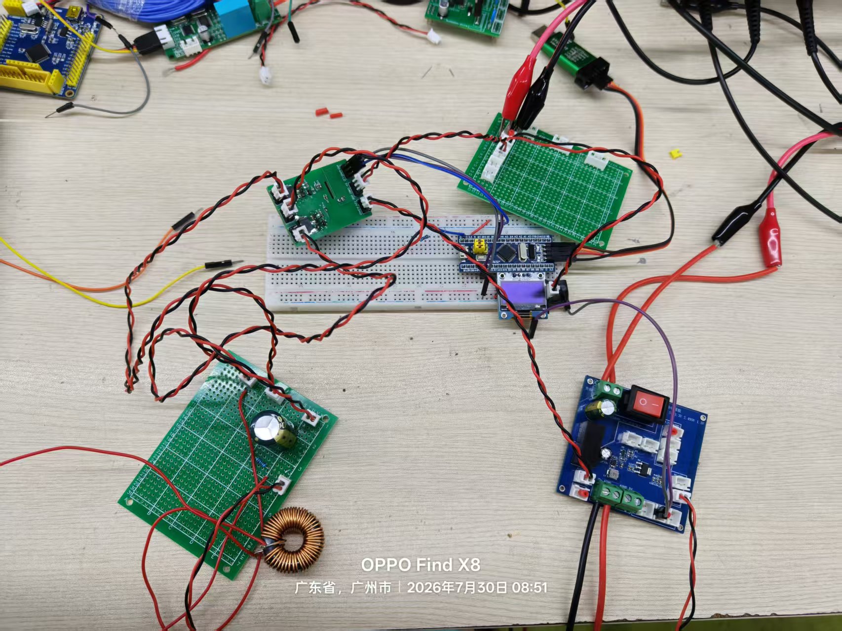
Also take a photo of your actual setup and how it’s connected!
Without pictures, it’s hard to explain and very difficult to analyze!
First, let’s correct two concepts:
1. “Independent power supply” ≠ “all grounds must be separated”
The UCC21520 already internally isolates the input side (GND) from the output low-side (VSSB). What you need to do externally is:
- GND → connect to your microcontroller signal ground
- VSSB → connect to your power ground AGND
- VDDA needs an isolated power supply, because VSSA is connected to VS (the switching node, jumping between 0 V and Vout), and a normal non-isolated power supply cannot handle it.
2. AGND and GND must not be connected with a resistor
If power ground and signal ground need to coexist, they must be shorted together with low impedance at one point (usually the negative terminal of the input filter capacitor). Connecting them with a resistor turns the ripple voltage from the switching current (ΔV = L×dI/dt) into noise on the signal ground, causing your PWM reference ground to bounce and distorting the drive waveform.
The direct cause of your current symptom:
“No PWM when the microcontroller is not connected, but no PWM after it is connected” → After the microcontroller is connected, the PWM signal line loses its reference ground. Most likely, the ground wire between the microcontroller development board and the UCC21520 board is not connected. Run a thick jumper wire to connect GND on both sides, and the symptom should disappear immediately.
If it still shows a few hundred millivolts after adding the jumper, check:
- Is the microcontroller PWM output push-pull?
- Is the microcontroller IO 3.3 V or 5 V? Driving the UCC21520 with 3.3 V (VCCI=5 V) is a marginal logic level; it’s best to use a unified 3.3 V supply or add level shifting.
Once the signal is connected, it gets pulled down to a few hundred millivolts. Focus on checking these three common pitfalls:
-
Check whether capacitors C6/C7 were mounted incorrectly: Your schematic shows 33 pF, so quickly confirm that the actual SMD parts weren’t mistakenly installed as 104 (100 nF) or even 1 µF. If large capacitors were used, the high-frequency PWM will be effectively shorted to ground as an AC signal.
-
Driver chip input pins (INA/INB) may be damaged by ESD: Disconnect the MCU wiring and power off the board. Use a multimeter in diode-test mode to measure the voltage drop from pins 1 and 2 of the chip to pin 4 (GND). If both forward and reverse readings are a few tenths of a volt or show a short, the chip inputs have likely been damaged by electrostatic discharge.
-
The right way to look at the waveform: Clip the oscilloscope probe’s ground lead to the MCU GND, and touch the probe tip to pin 1 of the UCC21520 (INA). First make sure you can see a clean 3.3 V/5 V square wave at the chip input. If there’s no signal at the input, everything downstream is obviously dead.
If the MCU outputs a clean PWM alone but dies when plugged into the driver board, check these hardware bugs:
-
Check C6 and C7 capacitors: Your schematic specifies 33pF for C6/C7. Double-check if you accidentally soldered 100nF (104) caps instead. A large filter cap will act as a short circuit to GND for high-frequency PWM signals.
-
Damaged IC Input Pins: Measure Pin 1 (INA) and Pin 2 (INB) with respect to Pin 4 (GND) using a multimeter in diode mode (board unpowered). If it reads near 0V, the driver’s internal ESD diodes or logic gates are shorted.
-
Proper Scope Probe Technique: Clip the probe’s ground lead directly to the MCU GND, then probe Pin 1 (INA) of the UCC21520. Verify if the square wave reaches the chip pin before troubleshooting the output side.
Sorry, this is my first time posting a help request on this forum, so I’m not quite sure how to ask for help ![]()
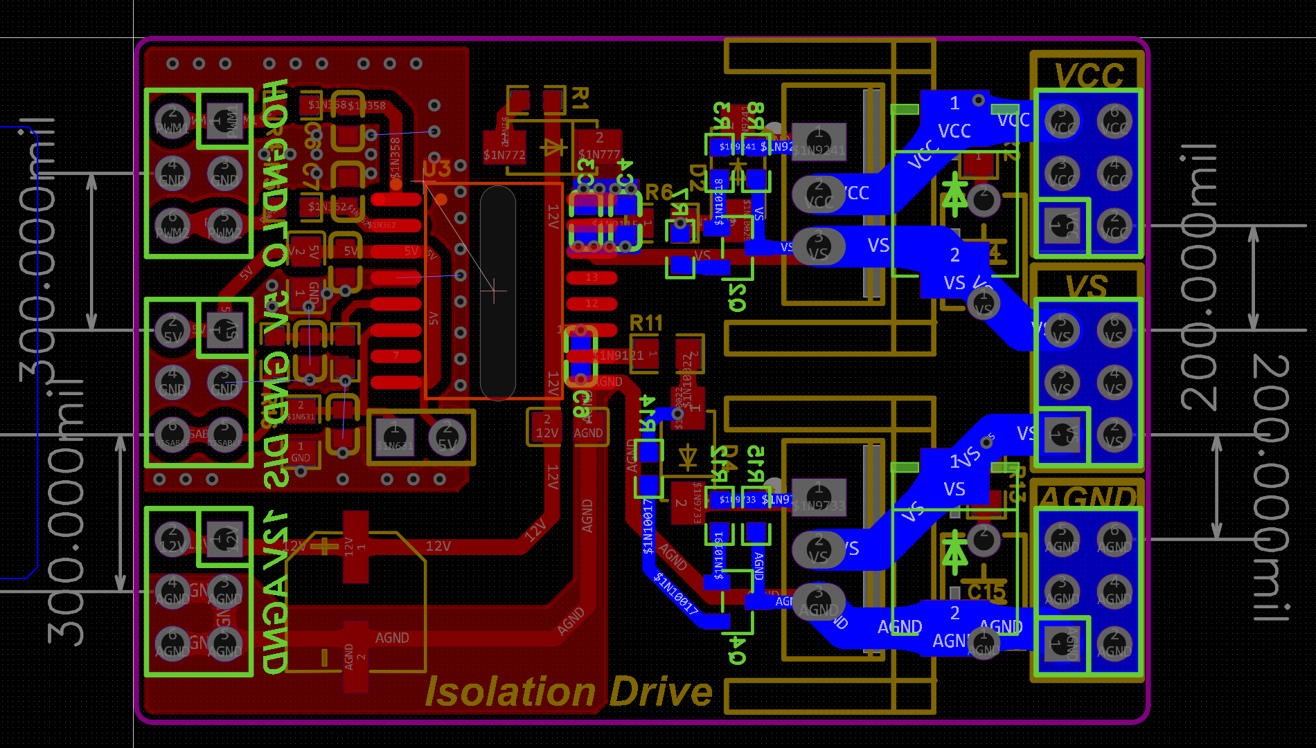
P1 is the PCB of this board, P2 is the wiring diagram. The bottom right is the auxiliary power supply, connected to 30 VDC, outputting 12 V and 5 V as the Boost input; the bottom left has the Boost inductor, output capacitor, and load resistor (1k); the top left is the board, and the MCU’s 5 V power supply is separate from the auxiliary power supply’s 30 V. The MCU is configured to output a pair of complementary PWM signals (blue and purple Dupont wires) connected to this board.
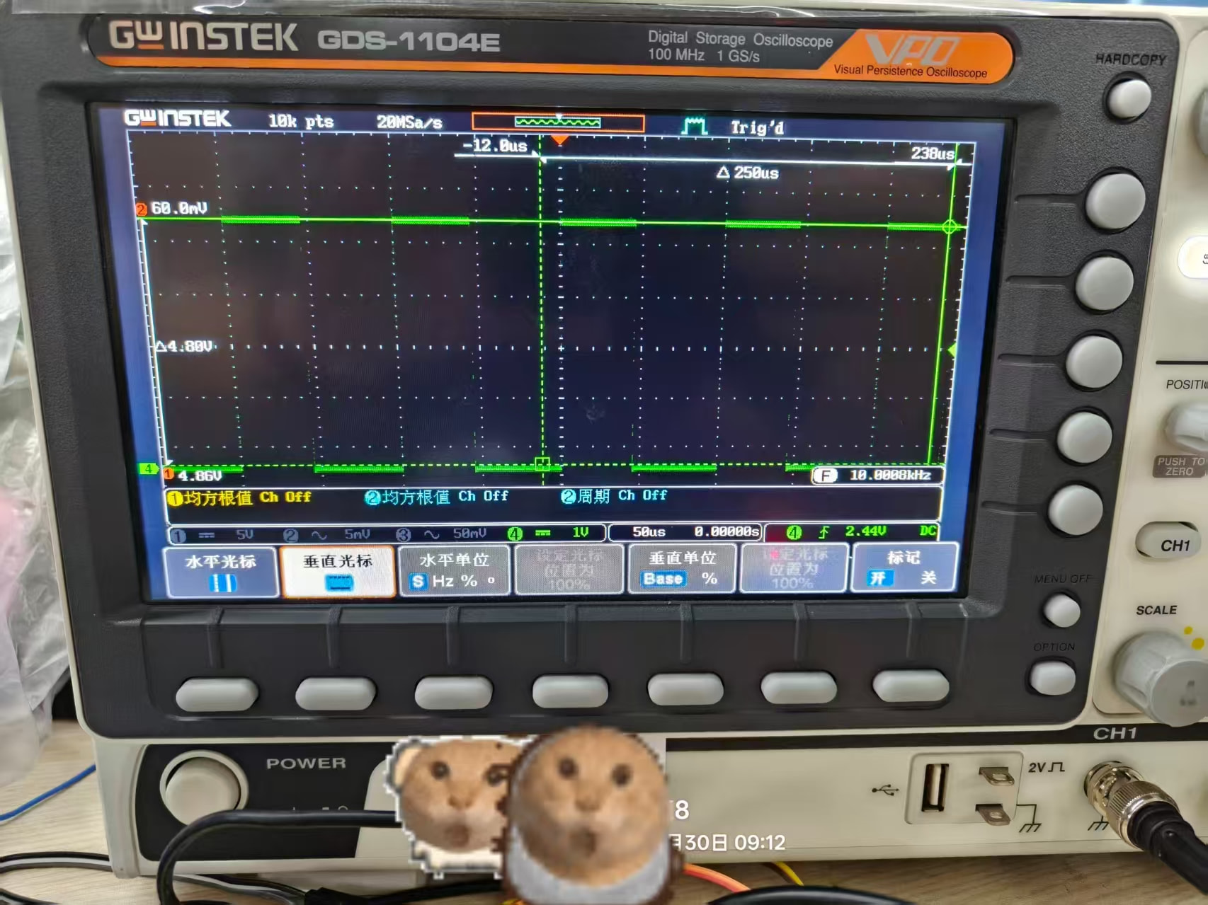
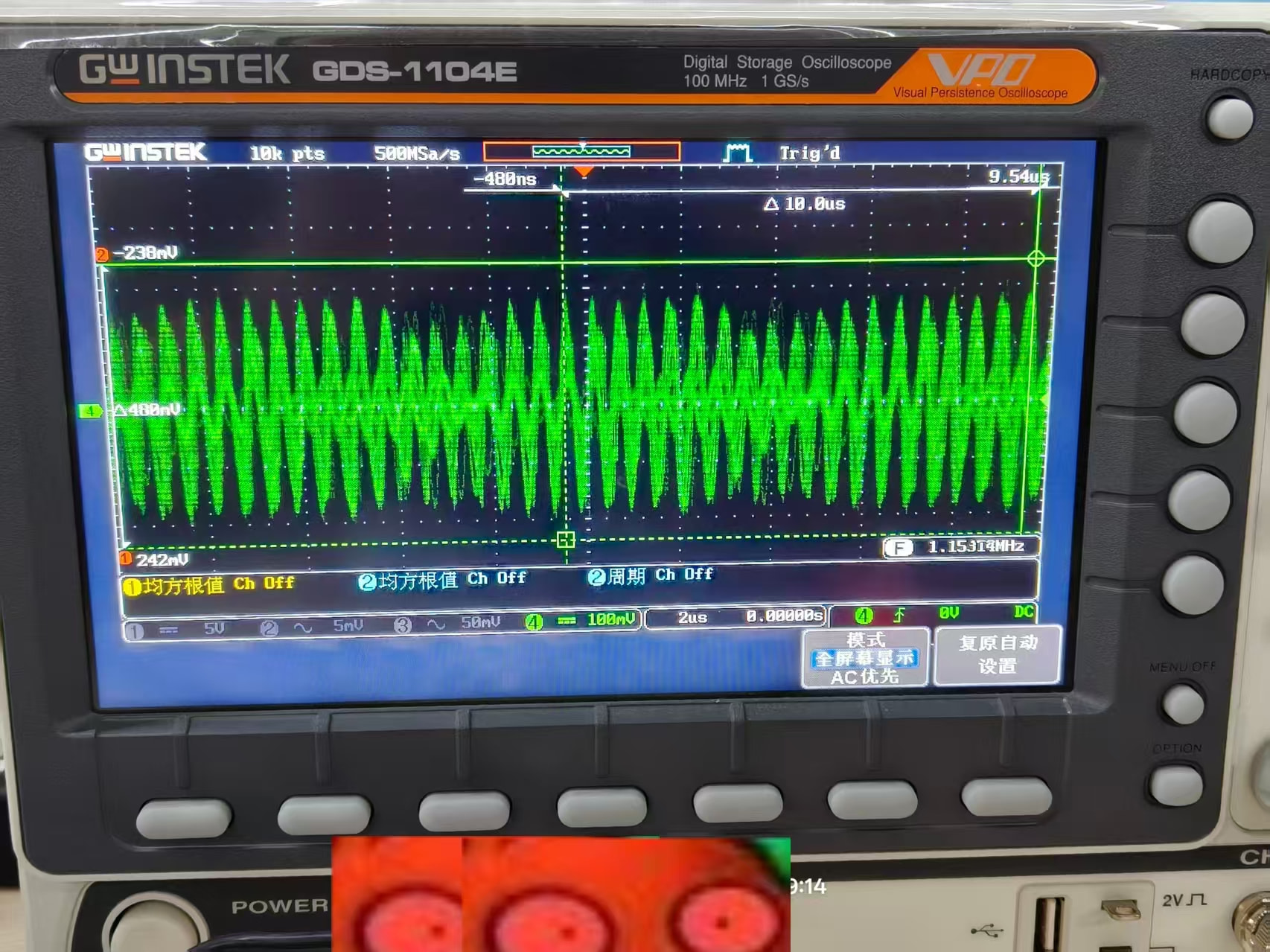
The first of the two images above shows the MCU PWM output not connected to the board. If I turn on the MCU’s 5 V supply first without turning on the auxiliary power supply, then connect the PWM directly to the board, and then turn on the auxiliary power supply, the PWM waveform does not disappear; the displayed gate voltage of the low-side switch is as shown in the second image.
If I connect all the wiring first, then turn on the MCU’s 5 V supply, there is no PWM output at that point, and turning on the auxiliary power supply also produces no output.
The oscilloscope and the specific diagrams have been placed on the 14th floor ![]()
This gate waveform doesn’t look quite right. It seems like noise—the half-bridge driver IC isn’t working.
You triggered a power-up sequencing violation that is clearly marked in red in the UCC21520 datasheet.
The input pins of the UCC21520 (INA/INB) have internal ESD protection diodes connected to VCCI. When your auxiliary supply is off, VCCI = 0 V, and the MCU PWM high level will inject current into VCCI through the ESD diode. If the signal remains applied (the wires are connected first), the internal parasitic SCR structure of the chip is triggered and enters latch-up — the input pin is pulled low-impedance to ground, effectively shorting the MCU PWM pin to ground, so of course it cannot output.
The reason that “powering the MCU first and then plugging in the wire” works is that the moment the Dupont wire is connected, the contact bounces, so the latch-up condition is not sustained and the chip does not get latched. The auxiliary supply then powers up, VCCI is established normally, and everything is OK.
What you need to do now is ensure the power-up sequence: the auxiliary 30 V supply (→ 5 V/12 V) must stabilize first, and only then should the MCU output PWM.
The simplest hardware fallback is: connect the DIS pin (pin 3) in your schematic to an MCU GPIO. During MCU initialization, pull DIS high first (disable the driver), wait 100 ms after the auxiliary supply has stabilized, then pull DIS low to enable the output. This way, even if the timing is wrong, the chip remains disabled and will not latch up.
Also, changing R14/R15 from 1 kΩ to 4.7 kΩ will greatly reduce the current injected into the MCU during latch-up.
The observed behaviour is characteristic of CMOS latch-up induced by violating the recommended power sequencing.
When the PWM lines are connected before VCCI is established, the ESD protection diodes at INA/INB become forward-biased. Current flows from the MCU IO pin through R14/R15 into the VCCI pin, charging the local decoupling capacitors. The resulting potential at VCCI (typically 1–2 V) is insufficient for normal operation but sufficient to bias the parasitic bipolar structures inherent in the IC process. This initiates a regenerative latch-up condition, creating a low-impedance path from the input pin to ground. The MCU output stage sees an effective short, and the observed voltage collapses to the resistive divider level across R14/R15 (hence the few-hundred-millivolt reading).
The plug-in-after-powering scenario avoids sustained latch-up because the mechanical contact bounce of the Dupont connector interrupts the bias condition before it can regenerate. Once the auxiliary supply is subsequently enabled, VCCI rises monotonically from 0 V and the device initialises correctly.
Required corrective actions:
- Enforce power sequencing: The auxiliary supply providing VCCI and VDDB must reach regulation before PWM signals are applied.
- Hardware disable: Route the DISABLE input to a microcontroller GPIO. Assert high during startup; release only after confirming auxiliary rails are stable.
- Current limiting: Increase R14 and R15 to 4.7 kΩ to reduce latch-up current magnitude.
- Firmware guard: Implement a post-boot delay before PWM module enablement.
Yes, it probably isn’t working. The two people downstairs might be AI, but what they said makes sense. I’ll try controlling it by connecting the auxiliary power first and then applying the microcontroller control. Thanks, expert.
Is it okay to turn on the auxiliary power supply first without turning on the microcontroller power supply?
DIS is soldered directly to signal ground.