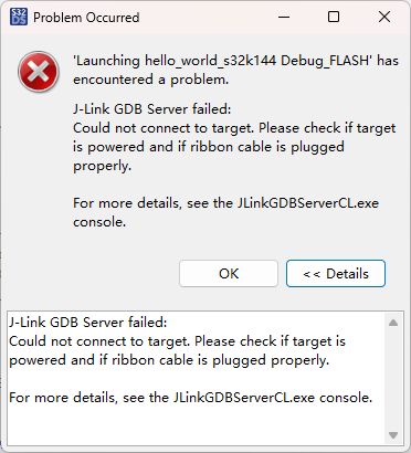
The new board has arrived, but I can’t flash it this time. Here’s the log:
SEGGER J-Link GDB Server V9.72 Command Line Version
JLinkARM.dll V9.72 (DLL compiled Aug 26 2026 14:38:37)
WARNING: Unknown command line parameter -RestoreRAMOnDownload found.
WARNING: Unknown command line parameter 0 found.
Command line: -if swd -device S32K144 -endian little -speed 500 -port 2331 -swoport 2332 -telnetport 2333 -vd -ir -localhostonly 1 -singlerun -timeout 0 -nogui -RestoreRAMOnDownload 0
-----GDB Server start settings-----
GDBInit file: none
GDB Server Listening port: 2331
SWO raw output listening port: 2332
Terminal I/O port: 2333
Accept remote connection: localhost only
Generate logfile: off
Verify download: on
Init regs on start: on
Silent mode: off
Single run mode: on
Target connection timeout: 0 ms
------J-Link related settings------
J-Link Host interface: USB
J-Link script: none
J-Link settings file: none
------Target related settings------
Target device: S32K144
Target device parameters: none
Target interface: SWD
Target interface speed: 500kHz
Target endian: little
Connecting to J-Link…
J-Link is connected.
Firmware: J-Link LPCXpresso V2 compiled May 2 2023 17:39:56
Hardware: V1.00
S/N: 724304970
Checking target voltage…
Target voltage: 3.30 V
Listening on TCP/IP port 2331
Connecting to target…
ERROR: J-Link script file function InitTarget() returned with error code -1
ERROR: Could not connect to target.
Target connection failed. GDBServer will be closed…Restoring target state and closing J-Link connection…
Shutting down…
Could not connect to target.
Please check power, connection and settings.
Type “connect” to establish a target connection, ‘?’ for help
J-Link>connect
Please specify device / core. : S32K144
Type ‘?’ for selection dialog
Device>
Please specify target interface:
J) JTAG (Default)
S) SWD
T) cJTAG
TIF>S
Specify target interface speed [kHz]. : 4000 kHz
Speed>
Device “S32K144” selected.
Connecting to target via SWD
ConfigTargetSettings() start
ConfigTargetSettings() end - Took 15us
InitTarget() start
SWD selected. Executing JTAG → SWD switching sequence.
Connect Under Reset
SWD selected. Executing JTAG → SWD switching sequence.
Communication error while accessing MDM-AP.
Connect Under Reset
InitTarget() end - Took 409ms
Connect failed. Resetting via Reset pin and trying again.
ConfigTargetSettings() start
ConfigTargetSettings() end - Took 13us
InitTarget() start
SWD selected. Executing JTAG → SWD switching sequence.
Connect Under Reset
SWD selected. Executing JTAG → SWD switching sequence.
Communication error while accessing MDM-AP.
Connect Under Reset
InitTarget() end - Took 406ms
****** Error: J-Link script file function InitTarget() returned with error code -1
Error occurred: Could not connect to the target device.
For troubleshooting steps visit: https://kb.segger.com/J-Link_Troubleshooting
To start with, the logs this time have fundamentally changed compared with the previous two posts—in the first two, communication was still possible and the registers could be read; this time, the MDM-AP cannot even be accessed, so the debugger is blocked right at the chip’s door.
Let’s go through it point by point:
Communication error while accessing MDM-AP — The SWD debug protocol in the S32K1 series uses MDM-AP (Memory Debug Access Port) for the handshake, and accessing this AP is the first step in debug communication. Failure to access MDM-AP = the chip is not responding on the SWD bus at all: either the chip is locked up, the physical link is not working, or the debug port timing is off.
Connect Under Reset failed twice — J-Link already tried to connect while holding the chip in reset, avoiding interference from running code, but it still failed. This means the issue is not that “the program ran away and the debugger lost control”; rather, the chip and the debugger are fundamentally not communicating at the physical/protocol layer.
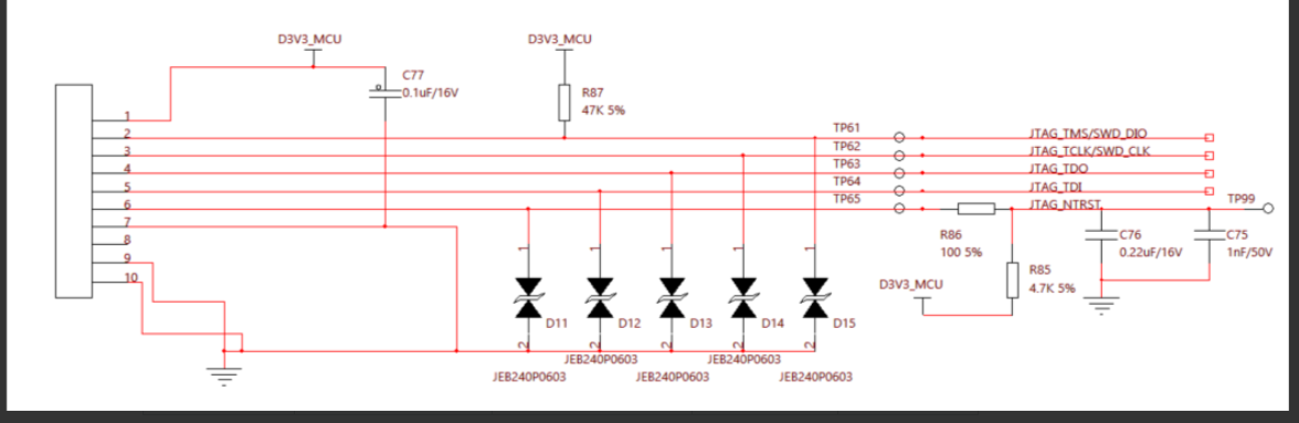
RESET is 0 V to ground — This time it differs from the 1 V in post 411. 1 V indicated an abnormal voltage divider; 0 V means RESET is being pulled to ground by the external circuitry. In your schematic, TP65 NTRST uses a reset path consisting of R86 100 Ω + C76 0.22 μF + R85 4.7 k pull-up to D3V3_MCU. When J-Link performs Connect Under Reset, it pulls NTRST low. If NTRST and RESET on your board are connected to the same node on the PCB (or if there is an internal NTRST→RESET path in the chip), then RESET being pulled low now makes sense.
J-Link LPCXpresso V2 — Note that you are not using a standard J-Link; you are using the V2 firmware from an onboard LPCXpresso debugger. LPCXpresso has the best compatibility with NXP’s own chips, but the S32K144 is not on its “native support” list, so the debug script may be incomplete.
Suggested troubleshooting order:
Disconnect the debugger USB, power the board on its own, and measure the RESET voltage (it should be 3.3 V, not 0 V). If it is still 0 V, check around the reset button / R86 / C76 area.
Check continuity from the SWDIO/SWCLK traces to the MCU pins (especially whether ESD diode D11–D15 are soldered backwards—reversed JEB240P0603 diodes can directly short the line).
Try 100 kHz using J-Link Commander.
Run unlock Kinetis + mass erase (if it can still get into connect).
Thanks for your reply. We found the cause the next day: the output of the power-management chip was shorted to ground, which cut off the downstream 3V3 supply.