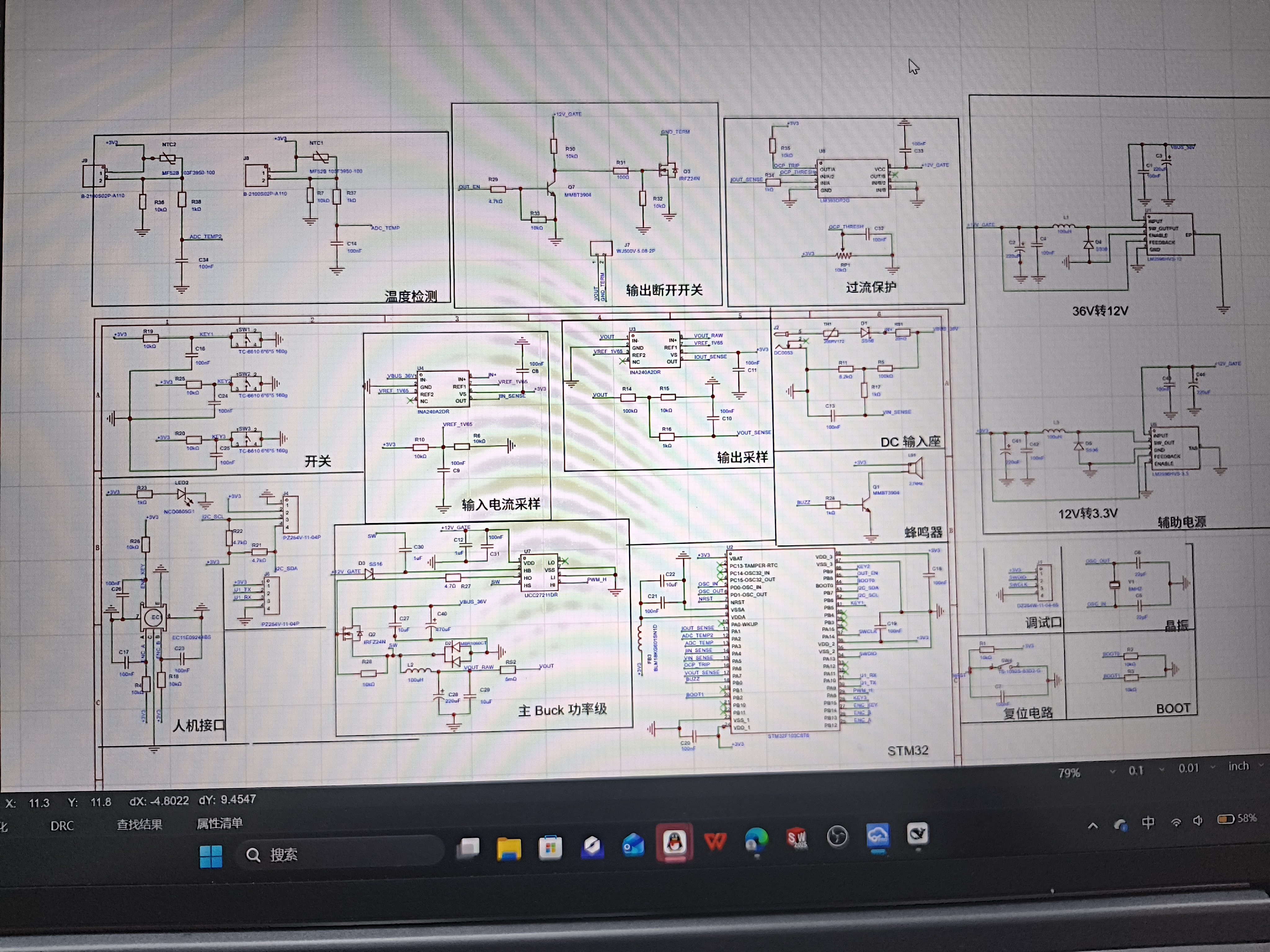
- No specific question, no thoughts or questions of your own? Just freeloading off others to have them do a full schematic review for you?
- The image isn’t even a screenshot—it’s this blurry. Don’t you even look at the picture after taking it? (Hint: EasyEDA has an export feature that can export schematic images/PDFs)
Recommended reading: https://bbs.eeclub.top/t/topic/109
Hey, I’ll bite — and I’m not trying to pile on, but that photo really is impossible to review. I can barely read the net names, let alone the component values.
If you want a real review, give people something to work with:
-
Export the schematic as a PDF or high-res PNG. In EasyEDA it’s literally File → Export — takes five seconds, and the output is readable.
-
Post your spec: input range (you wrote 36V, but what’s the absolute max, and any transients?), output voltage/current, efficiency target, why an STM32 instead of a dedicated buck controller, and whether you need isolation.
-
Run ERC first and clear the floating/single-pin nets, so nobody has to guess what’s a mistake and what’s intentional.
Then break it up — ask one concrete question per post. “Is my input current-sense topology OK?” or “is my gate drive safe?” will get you far better answers than dumping the whole sheet and asking “is this fine?”.
From what I can make out it’s a digitally controlled buck with input current sensing — nothing obviously wrong, but I genuinely can’t confirm any values. Repost a proper export and I’ll go through it block by block.
From what can be made out clearly, here are a few things that are “once the board is laid out, you can’t change them” and must be locked in before routing:
-
Main Buck hot loop: The input capacitor must sit right against the high-side MOSFET’s Drain and the low-side MOSFET’s Source; the smaller the loop area, the better. Keep the SW node copper as small as possible—don’t let it act as a transmitting antenna.
-
Current sensing (the input current sensing part): Use a Kelvin four-wire connection for the sense resistor; route the amplifier’s differential inputs with equal length and right along the resistor. Absolutely do not let the high-current ground pass through the sense point; keep the RC at the amplifier output as close as possible to the ADC pin.
-
Bootstrap capacitor: Its capacitance should be at least 10× the MOSFET’s total Qg, and make sure it can be fully recharged every switching cycle; don’t omit the small series resistor.
-
Dead time and Vgs: With bootstrap drive, make sure the high-side Vgs doesn’t exceed 20V; synchronous rectification must have dead time—if the high- and low-side switches conduct simultaneously, that’s fireworks.
-
DC bias derating: For that row of 36V MLCCs, never calculate capacitance by nominal value; a 50V X7R can lose more than half its capacitance at 36V. For the input, electrolytic + MLCC in parallel is recommended.
-
Ground: Keep power ground and signal ground separate, tied at a single point under the Buck IC; don’t connect the sense ground and ADC reference ground arbitrarily.
-
3V3 LDO: Linear step-down from 12V; first calculate power dissipation and package thermal resistance, and lay out heat-spreading copper if you can.
The image is too blurry to make out the specific part numbers. Start by checking against these points.