具体怎么说啊佬,没懂为啥不能空载开环
如果焊接方面没有问题的话,我看见ADC采集的输入输出电压电流不准确会不会是ADC处理数据的算法问题,因为我改了一下数值处理的一些代码,误差就没那么大了
自己去了解一下boost的原理吧,下面给你个AI回复:
简单来说,Boost(升压)变换器在空载(无负载)且开环(无反馈控制)的情况下运行,会导致输出电压无限上升,最终烧毁电容、开关管或二极管。
以下是深度解析其背后的物理逻辑:
1. 能量“只增不减”的累积效应
Boost 电路的工作分为两个阶段:
- 充电阶段: 开关管导通,电感 L 储能。
- 放电阶段: 开关管断开,电感 L 将储存的能量与电源 V_{in} 一起叠加,向输出电容 C 充电。
在正常带载情况下,电感每个周期传递给电容的能量,会被负载消耗掉,从而达到能量平衡。
但在空载情况下,负载电流为零。这意味着每个开关周期从电感“泵”进电容的能量无处可去。根据电容储能公式 E = \frac{1}{2}CV^2,能量不断堆积,电压 V 必然会节节攀升。
2. 数学模型的推导
在理想状态下(连续导通模式 CCM),Boost 变换器的输出电压公式为:
V_{out} = \frac{V_{in}}{1 - D}
(其中 D 是占空比)
- 开环状态: 意味着占空比 D 是固定不变的(例如 $D=0.5$)。
- 理想与现实的冲突: 理论公式是在“动态平衡”下成立的。但在空载时,由于没有电流输出,电路会进入断续导通模式 (DCM)。在 DCM 模式下,如果占空比固定且负载趋近于无穷大,理论上的输出电压会趋向于无穷大。
3. 灾难性的后果
由于实际电路中不存在“无限大”的电压,系统会由于达到物理极限而崩溃:
- 电容击穿: 输出滤波电容的耐压值(VDC)被超过,电容炸裂或短路。
- 开关管/二极管损毁: MOSFET 的 V_{ds} 或二极管的反向耐压被击穿。
- 反馈失效: 虽然你说是“开环”,但即使有反馈电路,如果反馈速度不够快或者没有设计过压保护 (OVP),在空载瞬间产生的电压尖峰也足以致命。
总结与预防措施
| 特性 | 表现 | 结果 |
|---|---|---|
| 能量传递 | 每个周期强制向输出端“泵”入能量 | 电荷在电容上不断堆积 |
| 电压反馈 | 缺失(开环),无法通过减小占空比来降压 | 电压失去约束 |
| 最终归宿 | 电压超过元器件耐压极限 | 硬件烧毁 |
实际工程中如何解决?
- 闭环控制: 使用 PWM 控制器,当检测到电压升高时,自动减小占空比 D。
- 假负载 (Dummy Load): 在输出端并联一个大电阻,确保即使在空载时也有微小电流消耗多余能量。
- 过压保护 (OVP): 增加硬件层面的电压钳位电路。
你提问的信息太少了,回答不了,没有图,没有数据,没有详细描述(做了什么修改?)…
基于STM32G474设计数字Buck-Boost电路的环路补偿参数,是一个从连续域(模拟)设计向离散域(数字)转化的过程。STM32G474 凭借其高分辨率定时器 (HRTIM) 和内置的数学加速器 (FMAC/CORDIC),非常适合这种高频数字电源控制。
计算和设计数字环路补偿参数通常分为以下几个关键步骤:
第一步:获取功率级的小信号模型 (s域)
首先,你需要知道被控对象(Buck-Boost功率级)的连续时间传递函数 G_{vd}(s) (控制到输出电压的传递函数)。
对于四管同步Buck-Boost,通常分为三种工作模式,其传递函数各不相同:
- Buck模式:属于最小相位系统,存在LC双极点和输出电容的ESR零点。
- Boost模式 / Buck-Boost模式:属于非最小相位系统,除了LC极点和ESR零点外,还存在右半平面零点 (RHPZ)。
- RHPZ 会导致相位延迟增加,同时幅值增加,极易引起系统不稳定。
- RHPZ 的频率公式通常为:f_{RHPZ} = \frac{R_{load} \cdot (1-D)^2}{2 \pi L}。
关键点:你的环路穿越频率(带宽) f_c 必须设计在最坏情况下的 RHPZ 频率的 1/5 到 1/3
以下,以保证足够的相位裕度。
第二步:设计模拟补偿器 (s域)
确定了 G_{vd}(s) 后,设定目标穿越频率 f_c (通常为开关频率 f_{sw} 的 1/10 )和相位裕度(通常为 45^\circ 到 60^\circ )。
- 电压模式控制 (VMC):通常需要 Type III 补偿器(PID等效,提供双极点和双零点),以补偿LC谐振带来的 180^\circ 相位掉落。
- 峰值电流模式 / 平均电流模式 (CMC):电流环将电感降阶为一阶系统,外环电压环通常只需要 Type II 补偿器(PI等效)。
假设使用 PI 控制器,其连续域传递函数为:
G_c(s) = K_p + \frac{K_i}{s}
第三步:离散化转换 (s域 → z域)
微控制器无法直接处理 s 域公式,必须将其离散化为 z 域。常用的离散化方法是双线性变换(Tustin变换),它能较好地保留频域特性。
代入 Tustin 变换公式:
s \approx \frac{2}{T_s} \frac{1 - z^{-1}}{1 + z^{-1}}
(其中 T_s 为控制环路的采样周期)
将上式代入 G_c(s),即可得到数字补偿器的传递函数 G_c(z)。
第四步:推导差分方程 (C语言实现)
将 G_c(z) 转换为时域的差分方程,这是 STM32G474 实际执行的代码逻辑。以标准的增量式 PI 控制为例,推导后的标准差分方程为:
\Delta u[n] = K_p \cdot (e[n] - e[n-1]) + K_i \cdot T_s \cdot e[n]
u[n] = u[n-1] + \Delta u[n]
- e[n]:当前ADC采样电压与基准电压的误差。
- e[n-1]:上一次的误差。
- u[n]:当前计算出的控制量(HRTIM的占空比比较值)。
- u[n-1]:上一次的控制量。
第五步:STM32G474 硬件增益标定
在数字系统中,你计算出的 K_p 和 K_i 不能直接套用模拟计算的结果,必须引入ADC量化增益和PWM转换增益:
- ADC增益 (K_{ADC}):例如使用12位ADC,参考电压为 3.3V,反馈分压比为 K_{div},则ADC采样值与实际输出电压的关系为:K_{ADC} = \frac{2^{12} - 1}{3.3} \cdot K_{div}
- PWM增益 (K_{PWM}):G474 的 HRTIM 分辨率极高(约 170ps)。如果 HRTIM 的周期寄存器值为 PER,则占空比与控制量的关系为:K_{PWM} = \frac{PER}{1.0}
最终写入 MCU 的参数 K_{p\_digital} 和 K_{i\_digital} 需要根据全局系统增益进行等比例缩放:
K_{digital} = \frac{K_{analog}}{K_{ADC} \cdot K_{PWM}}
STM32G474 编程优化建议
- 定点数运算:为了极速响应,尽量避免使用
float(尽管G474有FPU)。使用 Q15 或 Q31 格式的定点数,结合 CMSIS-DSP 库的arm_pid_q31函数,或者利用 G474 的 FMAC (滤波数学加速器) 让硬件自动计算 PI/Type III 补偿。 - ADC触发机制:使用 HRTIM 特定事件(通常是PWM周期的中心点)硬触发 ADC 采样,以避开开关噪声,这被称为“消隐”或平均电流采样。
谢谢大佬,原来如此啊
大佬,这个输入电流采样的两个输入端为啥这么接啊?这么接会导致输出电压是负值吧,可能是因为输入和输出电流流向不一样吗?规定输出电流为正,那么输入电流就是负的了?而且从同向输入端5号角看进去这个100欧电阻和6.2K的是并联关系呀,怎么理解呢,谢谢大佬
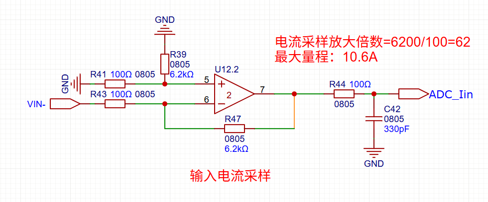
- 自己再细看一下电流流过采样电阻产生的电压正负方向
- 自己搜一下运放差分放大电路的原理和计算(模电基础)
我应该没记错呀,1.电流应该是VOUT+→负载→VOUT-→GND→VIN-→VIN+呀,2.差分运放的R47=R39,R43=R41的时候输出就是Vout=R47/R43(0-VIN-)呀。而且R41和R39合并后就是个反向放大了啊
兄弟,你对外部电流回路的理解稍微反了一下哦。电源是从 VIN 供电的,电流从 VIN+ 流入,经过电路后到达 GND,最后必须经过 R13 从 GND 流回 VIN- 才能回到外部电源负极。因为电流方向是 GND → VIN-,所以相对 GND(0V)来说,VIN- 处的电压其实是一个负电压!
既然输入信号是负压,运放采用的就是反相放大接法,输出 V_{out} = -62 \times (\text{负压}) ,负负得正,ADC 采样到的就是正电压啦。
至于你发现的 5 脚电阻并联,观察得很仔细!那是因为反相端(6脚)看进去的等效电阻是 100 欧和 6.2K 并联,为了消除运放输入偏置电流带来的误差,同相端(5脚)也必须接一个阻值相等的等效电阻接地。这在模电里叫平衡电阻,是为了提高采样精度的标准做法。
可是如果这样做的话从5角看出去这俩电阻就是并联的啊,并联后的等效电阻才是真正接入5角的
模拟电子技术基础学过没
开尔文走线了解一下
我突然懂了大佬!因为输入端采样电阻的电流是从GND流出来流到VIN-的,所以VIN-是个负值,负电压,所以正相输入端接GND(0V),反向输入端接VIN-,而上面的6.2K是差分放大的标准接法,只不过从形式上看这俩电阻都接地了,R41和R39好像是并联关系,所以说是反向放大好像也没啥问题
佬我想问一下,他这个供电方式不是有两种吗,一种是C口供电另一种是DC口供电,而且有电压诱骗芯片,并且三个配置引脚都给悬空了,默认诱骗20V,那也就是说供电只能拿个支持20V5A的100W充电器或者12V以上的带DC口的电源适配器给板子供电吗?
最高诱骗20V,不是只能诱骗20V,充电器不支持20V会降档,比如15V/12V
哦哦,也就是说诱骗芯片最高支持20V的电压档位,但是低于20V的也行,但是不能低于12V,要不然没法通过第一级的buck芯片降压出来12V给半桥驱动和小风扇供电
是的
对了佬,你做这个项目的时候有没有啥比较大的调试问题,能展开说一下吗,说几个比较大的或者容易犯的调试问题
__HAL_HRTIM_SETCOMPARE(&hhrtim1, HRTIM_TIMERINDEX_TIMER_D, HRTIM_COMPAREUNIT_1, PERIOD - CtrValue.BuckDuty);
// Boost占空比

\__HAL_HRTIM_SETCOMPARE(&hhrtim1, HRTIM_TIMERINDEX_TIMER_F, HRTIM_COMPAREUNIT_1, CtrValue.BoostDuty);
大佬为什么buck反向boost不用呢
为什么buckpwm 是period-buck
boost是boost呢
需不需要进行180度移相呢 已问过dpseek 不确定求解