I didn’t understand your question.
Source code is here
Still don’t understand what you’re asking.
Blogger, could you please help me? I modified the auxiliary power module, replacing your DCDC step-down module with the NDP2355KC module. My power inductor is the PSPMAA0605H-100M-ANP. However, I’m encountering issues: when I input 16V or similar voltages and try to set the output to around 10V, the system restarts (when powered via the C port) or activates overcurrent protection, immediately outputting maximum current (when using a regulated power supply). When using a DC power supply, the supply enters CC mode with an output voltage of around 6V. Additionally, the MOSFET on the board overheats significantly. Could you help analyze this issue? Thank you!
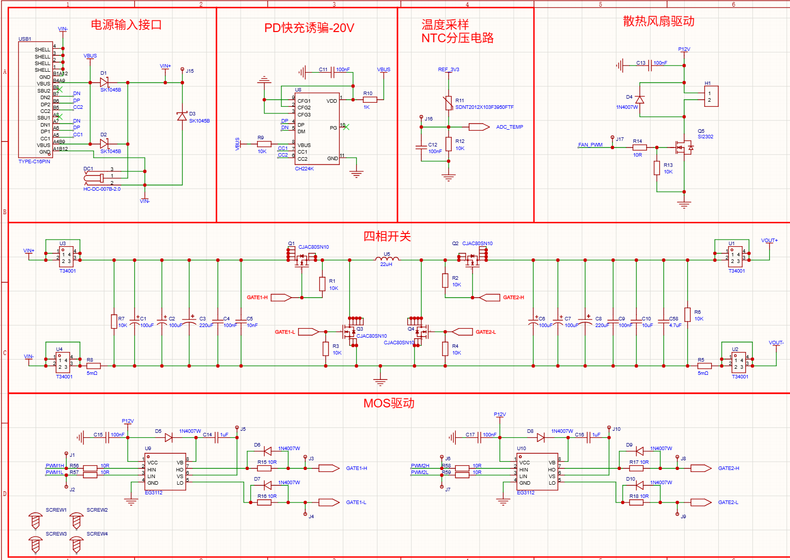
Check if there’s a short circuit at the output
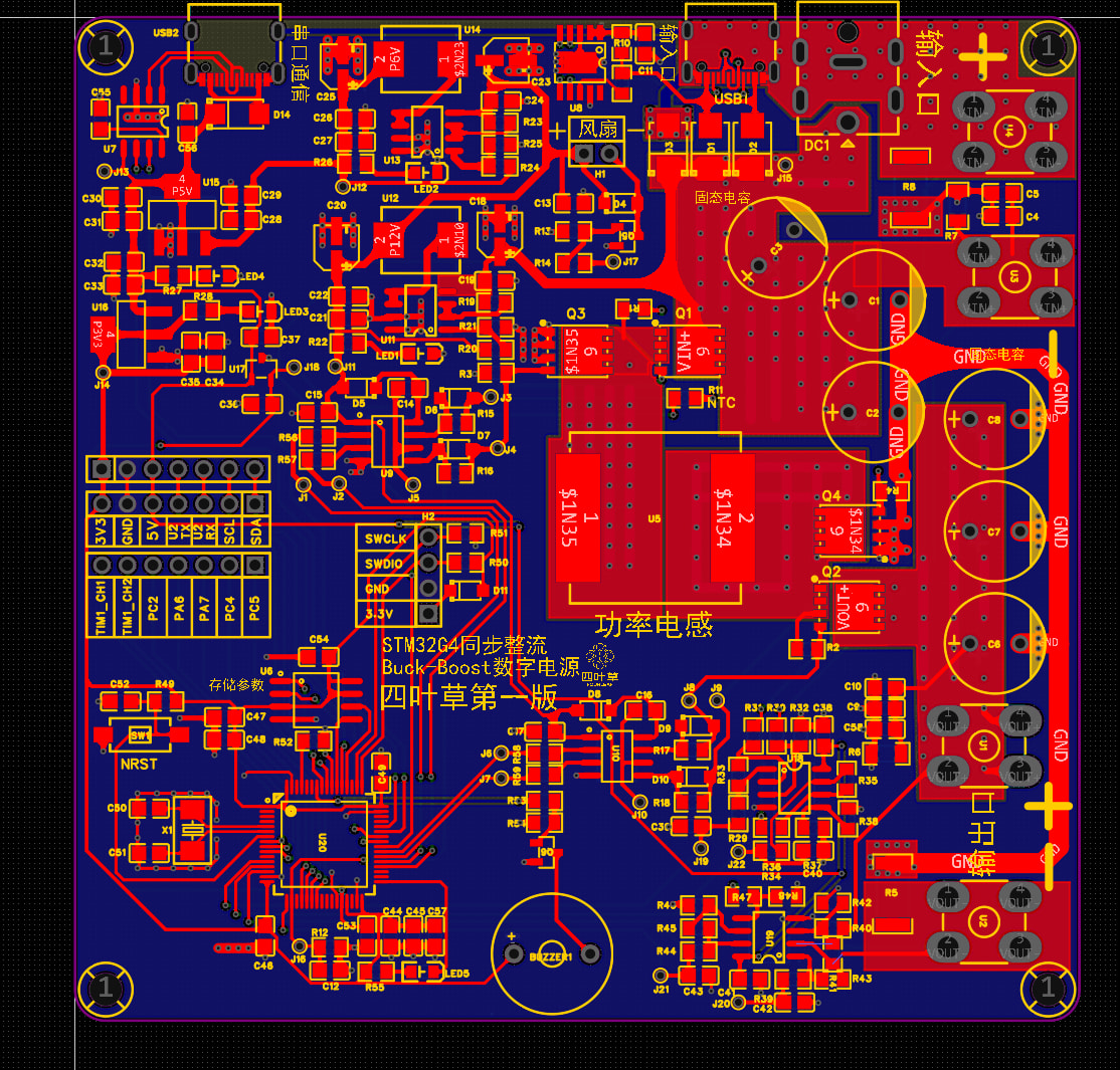
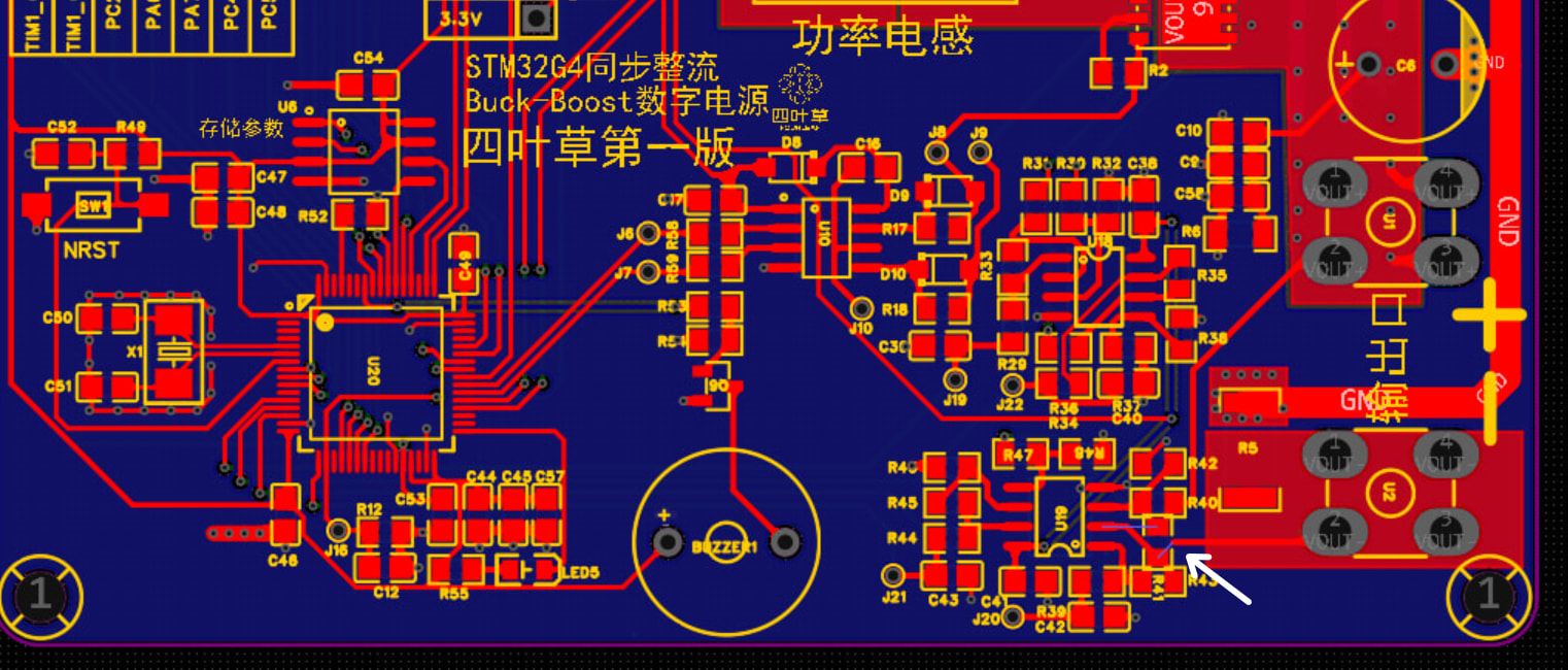
Take a look at your PCB layout
There is no short-circuit in the output either.
It’s just that the resistor was accidentally rotated slightly. The PCB is fine. I indeed didn’t notice that the current sensing should use Kelvin connections. Thanks to the blogger for the reminder.
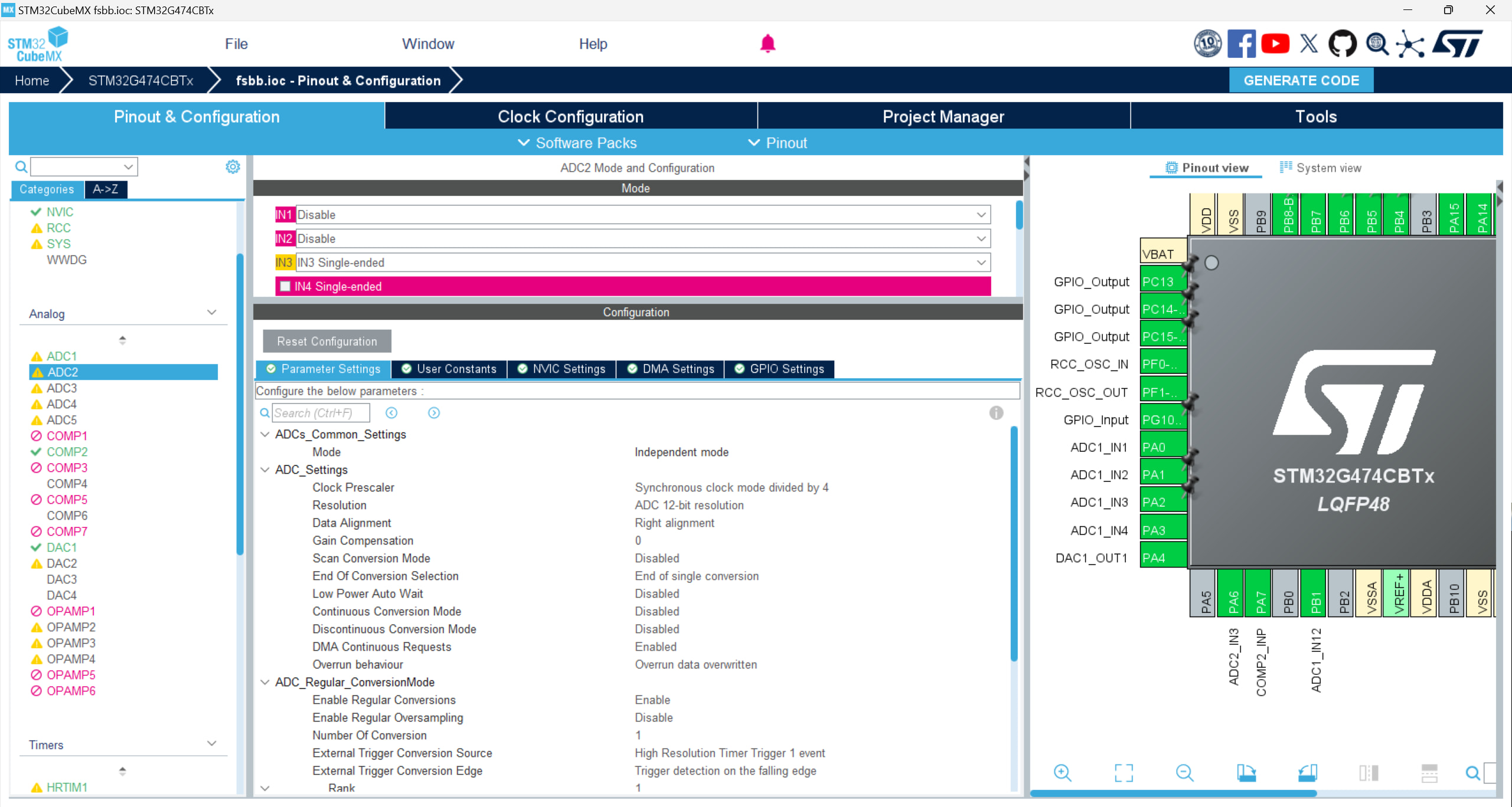
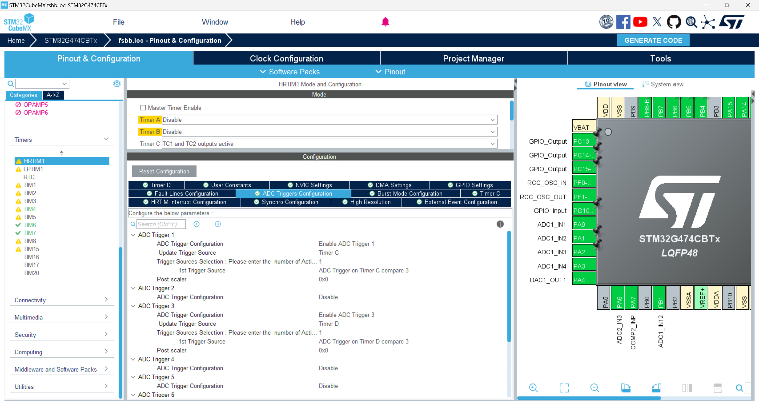
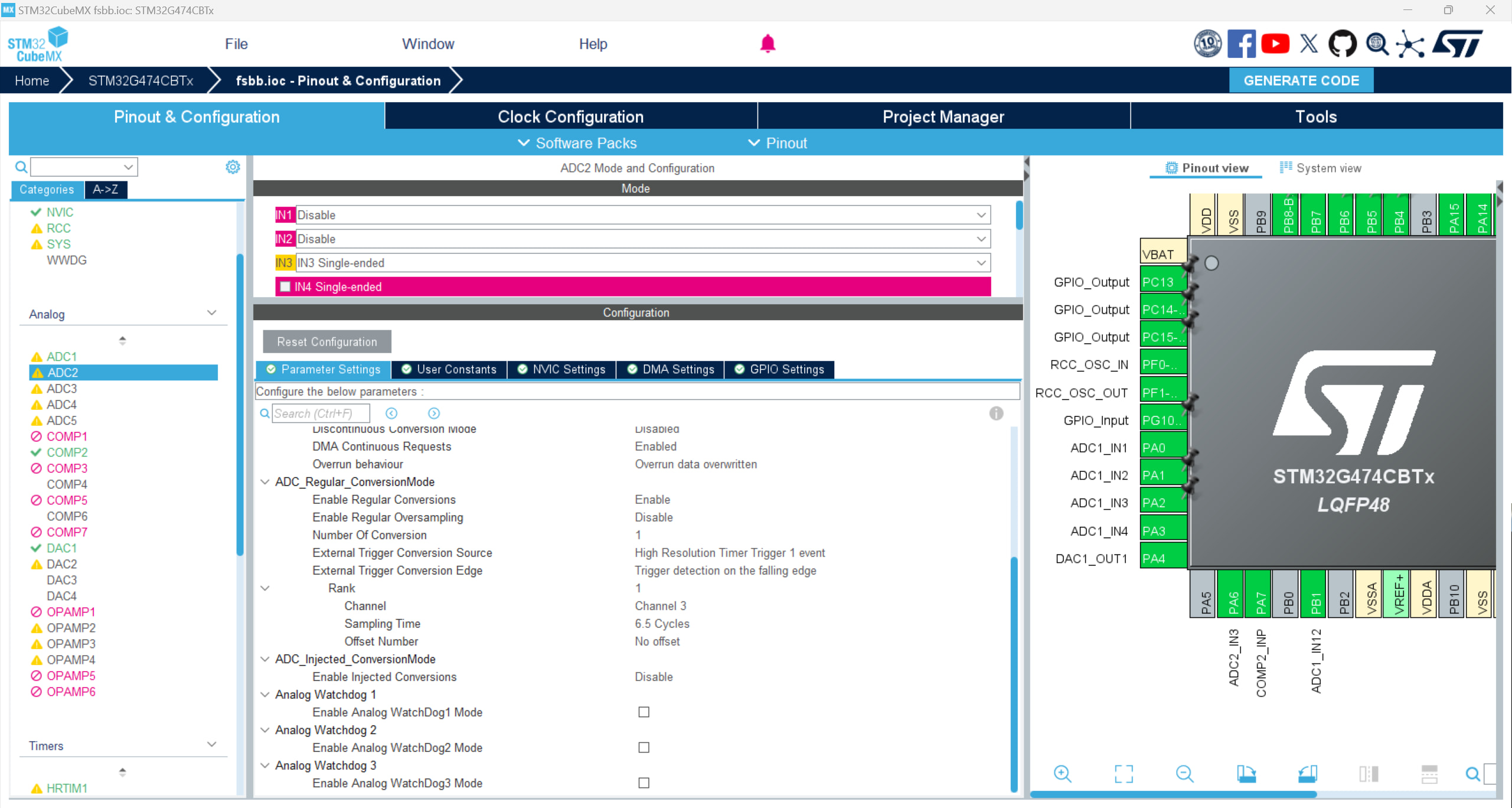
How do I configure this HRTIM to trigger ADC sampling at the center of the PWM period? I tried configuring it, but the trigger timing is off—it’s much later than what I set. How should I troubleshoot to find out where the problem is?
Show me a screenshot of how you set it up.
I only used C; D is for future expansion
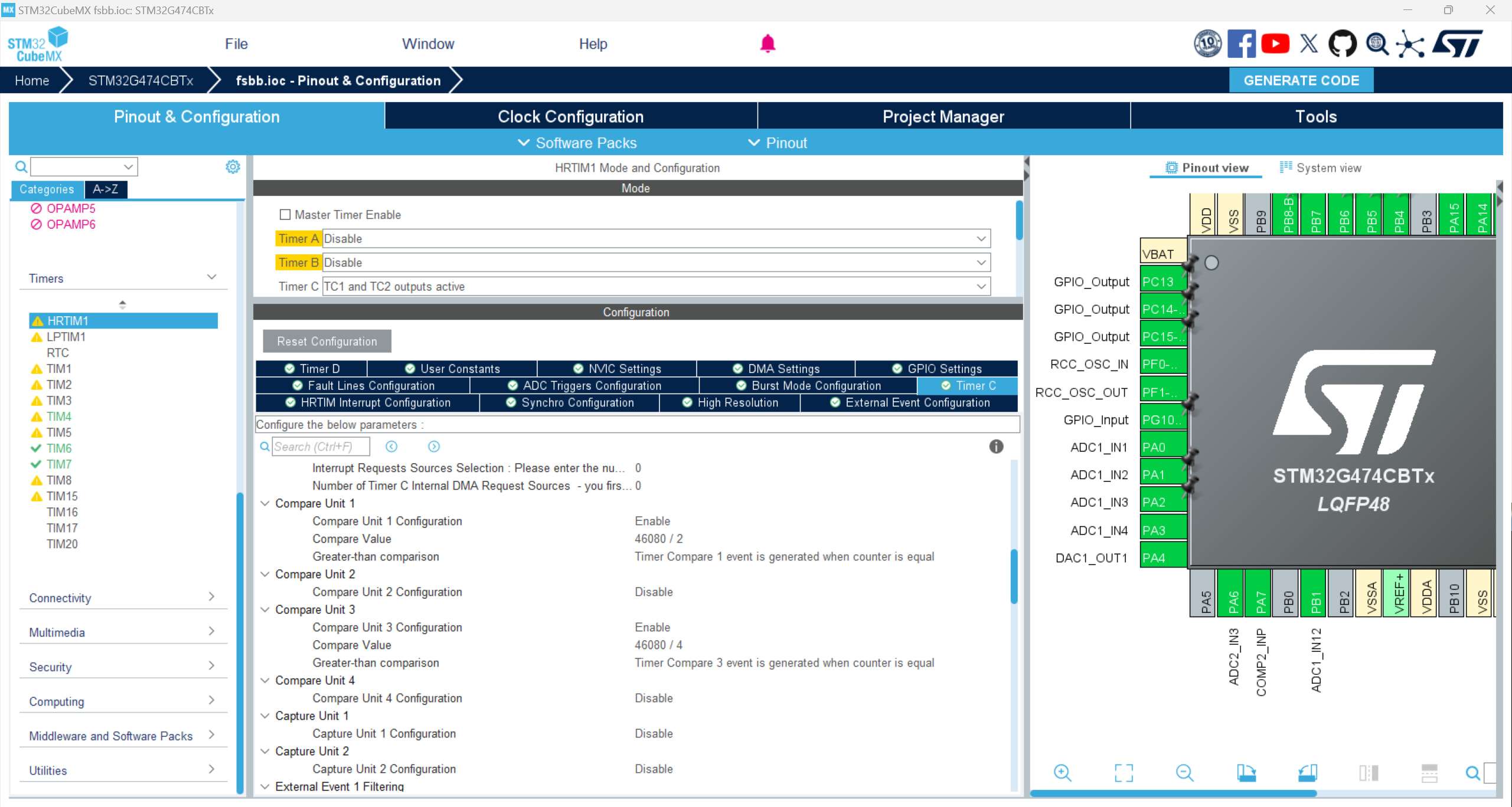
I found through testing that the moment my PC15 pin inverts is always 2.5uS later than the time I set. Here is my test function
// Callback function
void HAL_ADC_ConvCpltCallback(ADC_HandleTypeDef *hadc)
{
// ADC1_2_IRQHandler();

if (hadc->Instance == ADC2)

{

    GPIOC->ODR ^= GPIO_PIN_15;

    Control_Loop_Update(); // your high-frequency control loop

    // GPIOC->ODR ^= GPIO_PIN_15;

}

else if (hadc->Instance == ADC1)

{

    // GPIOC->ODR ^= GPIO_PIN_13;

    // flag_adc1 = 1;

    PID_V();

    GPIOC->ODR ^= GPIO_PIN_13;

}

// HAL_GPIO_WritePin(GPIOB, GPIO_PIN_15, GPIO_PIN_RESET); // pull low
}
I don’t know why the order in this screenshot got messed up ![]()
Bro, your testing method itself is flawed. By toggling the IO inside HAL_ADC_ConvCpltCallback, what you’re measuring isn’t the “trigger time” at all, but rather the “ADC sampling time + conversion time + interrupt response latency + the massive conditional checking overhead of the HAL library”.
Just take a look at the source code inside HAL_ADC_IRQHandler and you’ll see: ST’s HAL library checks a whole bunch of register states before calling this callback, so it’s completely normal for 1~2 µs to slip away in the process. Add to that the 6.5 Cycle sampling time configured in your screenshot, plus the 12.5 Cycles for conversion—that’s all real time being burned.
If you want to measure the actual trigger point, configure a timer output compare pin and use an oscilloscope to capture both the PWM signal and that compare output. If you absolutely must measure it inside an interrupt, ditch the HAL library. Go straight to the startup file, find the ADC interrupt entry, and toggle the GPIO on the very first line. You’ll find the latency drops significantly in an instant.
1 Like
I took a look at your CubeMX screenshot. Here are a few suspicious points you should check:
- Your ADC trigger source is configured as
Timer C Compare 3. I see that in your Timer C configuration, you set Compare 3 to46080 / 4. If your PWM period is 46080, shouldn’t the center point be/2? (Unless you are using center-aligned mode, in which case you’ll need to calculate it specifically). - Your ADC trigger edge is set to
Trigger detection on the falling edge. Are you sure the trigger event generated by the HRTIM is a falling edge where you expect it? Generally, the rising edge is the more common default configuration. - As the person above mentioned, 2.5µs is absolutely software overhead. With the G474 running at 170 MHz, 2.5µs is enough to execute over 400 instructions, all wasted on entering the interrupt, context saving, and the HAL library’s if checks. I recommend using DMA, letting the ADC directly trigger a DMA transfer once sampling is complete, rather than using a CPU interrupt to wait.
1 Like
Right, I did some more testing later and found that by putting it into the ADC1_2_IRQHandler function, the delay is practically gone.
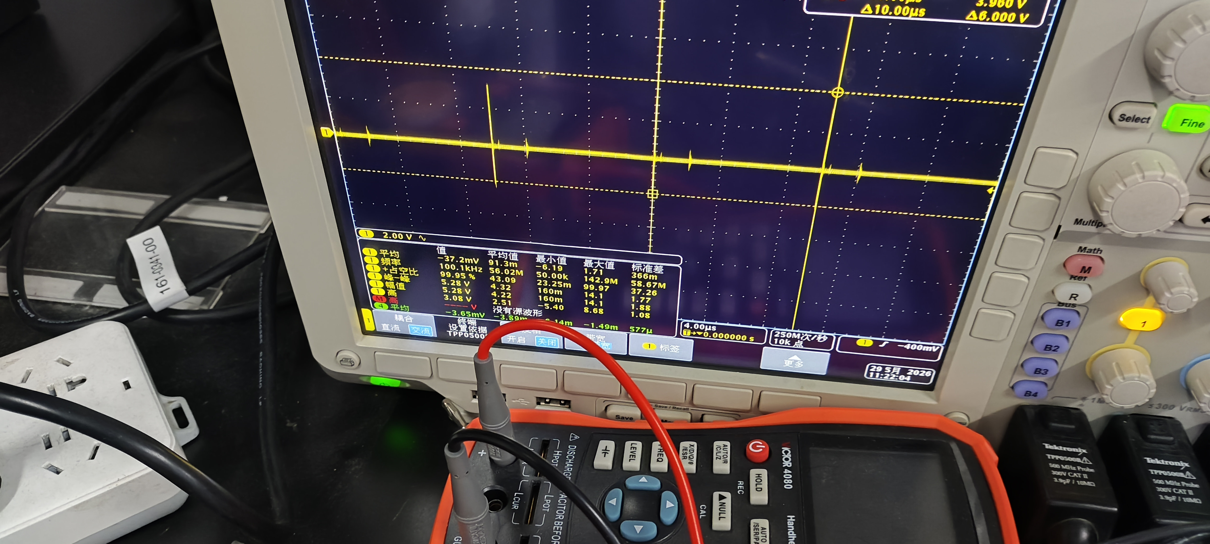
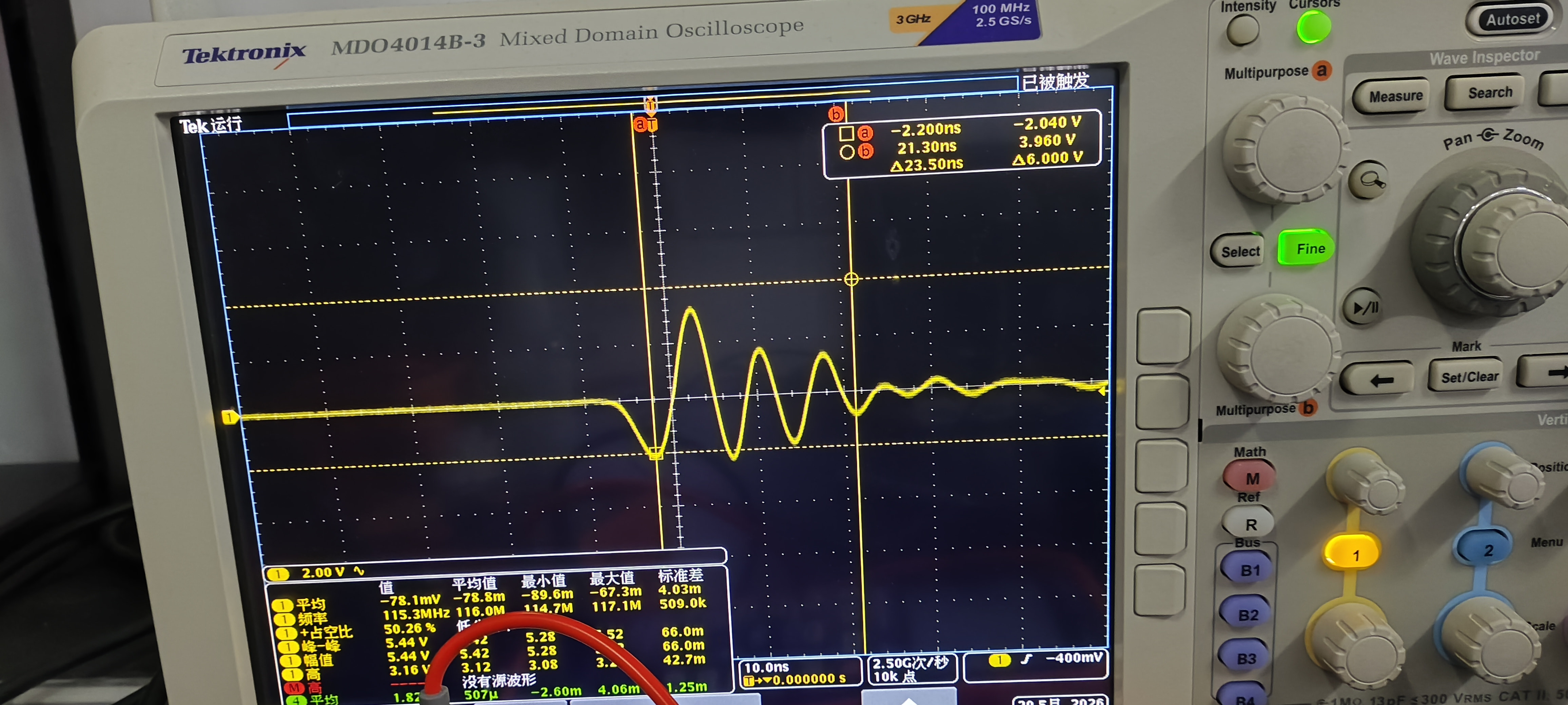
Hey guys, I’m currently in the testing phase. Initially, the functionality was normal (the output ‘ripple’ was very large, matching my switching frequency but amplified, and its frequency was very high, as shown below). Later, I added a few output capacitors, and upon powering it back on, the STM32’s ADCs seem to be completely dead. Now, the data measured from the ADC pins is exactly the same regardless of the external input. What could be the cause of this? My input voltage is 40V, the output is set to 30V, and the load is 20R. I want to ask if I need to add a component after the test module to protect the STM32 pins? If so, does anyone have any recommendations? Thanks guys!
I don’t get what you’re saying, is this my open-source board?
The topology is the same, it’s just that I drew this one myself
My questions are
-
In my plot of the output AC component, why does this very tall spike appear? It occurs 4 times within a single switching cycle; how can I eliminate its effect?
-
While testing the board, the ADC section of the STM32 completely died. I don’t know why the ADC part would get damaged; I even have an RC low-pass filter in front of the ADC pin, yet the ADC pin still got fried. What could be causing this? In my previous question, I suspected the ADC pin was damaged, and now I’m basically certain it’s really dead. (I’m guessing that the spike in the AC component shown in the plot above was too high, which caused my STM32’s ADC pin to get damaged—I don’t know if my guess is correct.) I’ve already killed two MCUs, both due to ADC pin damage, but I can’t find the root cause
-
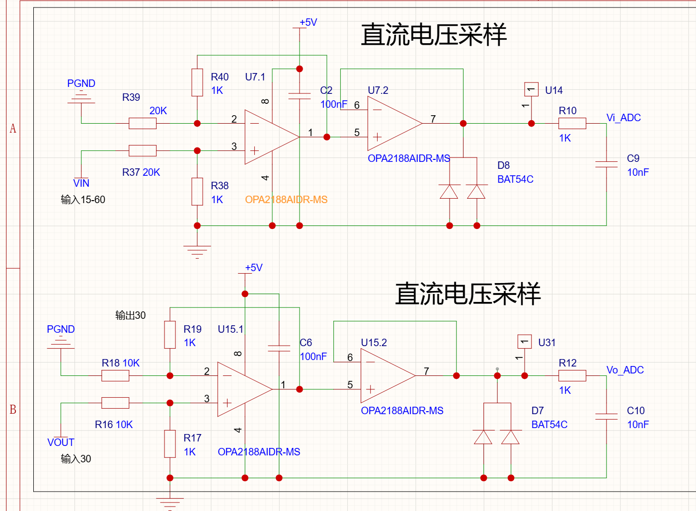
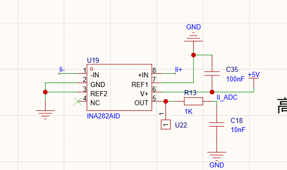
If I want to add extra protection to the STM32’s ADC pin to keep the ADC input between 0-3.3V, are there any good methods or components?
-
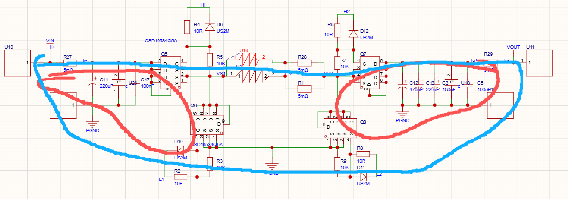
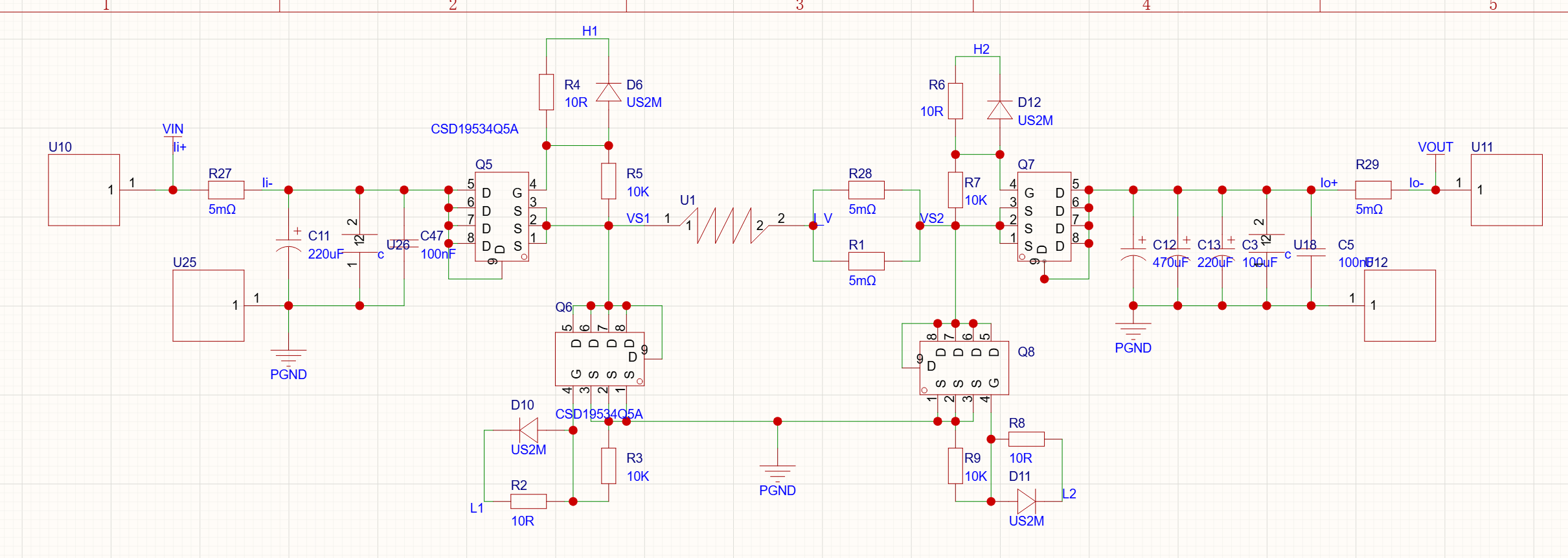
When doing the layout, should I minimize the entire loop from input to output (the blue lines)? Or is it enough to just minimize the two hot loops (the red lines) and not worry about the larger loop?
As shown in the image