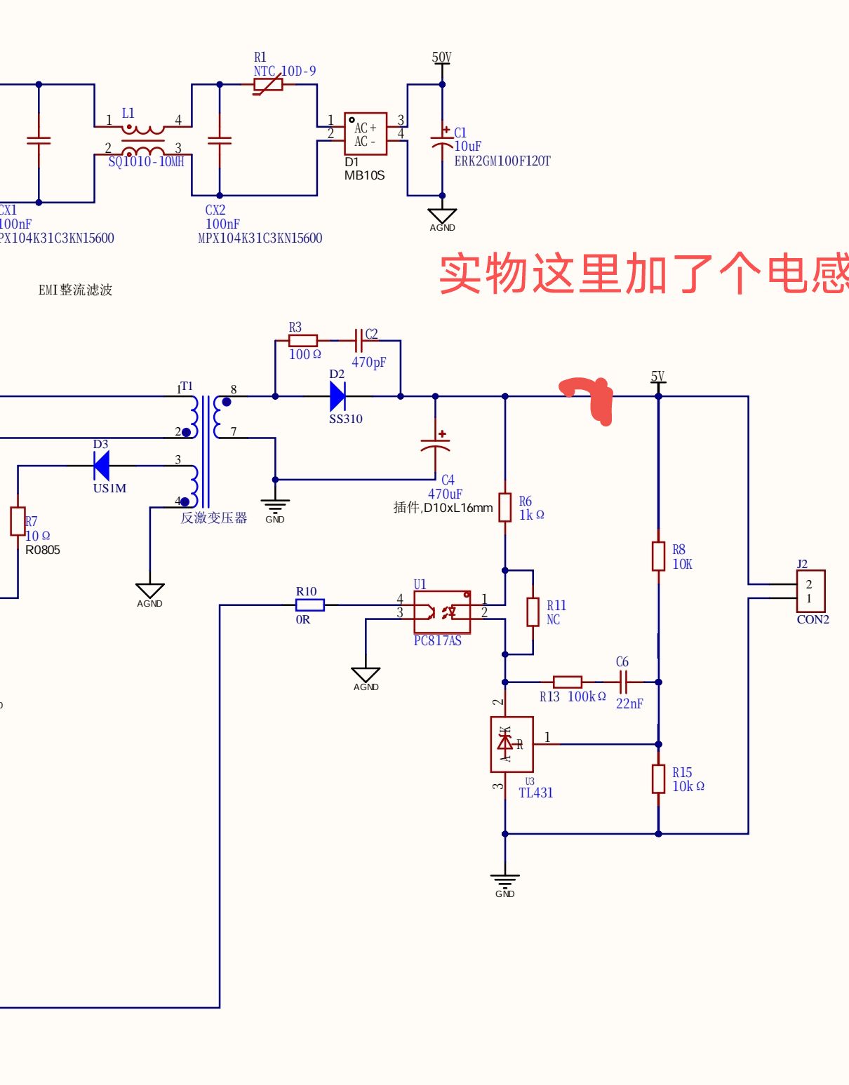
反激开关电源输出端V+前面为啥要加一个电感,一般不只是正激输出端才有电感的么? 有点懵

Morning, got a question for the experts here: why is there an inductor in front of the V+ terminal on the secondary side of a flyback SMPS? I thought only forward converters needed an output inductor. Kinda confused.

All the schematics I find online show flybacks without an output inductor.

But every flyback supply I’ve torn apart has one.

You can check out Teacher Sun the Engineering Guy’s Bilibili videos on flyback power supplies—he covers it there and mentions it’s for filtering.

It’s for ripple suppression.

好像是哎 :thinking:

In the design of a DC-DC + LDO voltage-regulator module, an inductor is also placed in between—its sole purpose is to suppress ripple.

We can reserve space for later and try adding an inductor to compare the effects with and without it.

Thanks for the insight :+1:

Hello! This question does confuse many newcomers to power-supply design. Put simply, an output inductor is not a fundamental requirement of the flyback topology, but it is often added in real products to optimize performance.

1. Basic principle: why a flyback usually “doesn’t need” an output inductor

In an ideal flyback converter the transformer itself acts as the inductor—energy is stored in the primary winding and released through the secondary. Only a rectifier diode and an output capacitor are required to transfer energy and smooth the voltage. This is the structure you see in most textbooks and schematics.

A forward converter is different: its transformer only transfers energy, it doesn’t store it, so an output inductor (freewheeling choke) must be added to keep the current continuous and smooth the output.

2. Practical optimization: why real products add an inductor

The part you saw while tearing a unit down is usually a small bead or a common-/differential-mode choke. It serves the following purposes:

  • Suppress high-frequency noise and ripple: the secondary current in a flyback is pulsed, creating large switching-frequency ripple and HF noise across the capacitor’s ESR. Adding an inductor (L) with the output capacitor (C) forms an LC filter that strongly attenuates these components, yielding a cleaner DC output. This is vital in low-noise applications (audio gear, precision instruments).

  • Improve electromagnetic compatibility (EMI): switching-node HF noise can radiate out through the output cable and cause EMI-test failures. An inductor—especially a common-mode choke—blocks this noise from reaching the load, helping the product pass strict EMC regulations [[5]].

  • Mitigate diode reverse-recovery issues: in some designs the small inductor limits the di/dt during diode reverse recovery, reducing oscillation and voltage stress and improving efficiency and reliability.

Summary:

Think of it this way:

  • Schematics show the minimal core architecture needed for function.
  • Real products add many optimization and compensation circuits to meet reliability, stability, EMI regulations, and user-experience demands. That output inductor is one such “nice-to-have” component added to make the supply both “usable” and “compliant.”

So your observation is spot-on! Online schematics give the “standard answer,” while the supply you dismantled shows “best practice.” It illustrates the journey from theory to engineering reality.

Thank you, experts. I’ve learned a lot. Much appreciated.