Bro, hello! When recreating the classic power supply problem from the national electronics competition, encountering such “mystical” issues is totally normal—this question was a notorious pitfall that tortured many people back in the day. For switch-mode power supply analog circuits, especially current sharing in parallel configurations, layout, routing, and interference are often far more critical than the schematic itself.
Based on your provided schematic, observed phenomena, and MCU replacement situation, let me help you analyze each aspect step by step to clarify your thinking:
1. About the INA199A1 Gain “Randomly Changing” and the 0.2mV Reading
You mentioned: at 0.2A current, you measured only 0.2mV across the shunt resistor, and the gain appears unstable.
There’s a clear Ohm’s Law contradiction here:
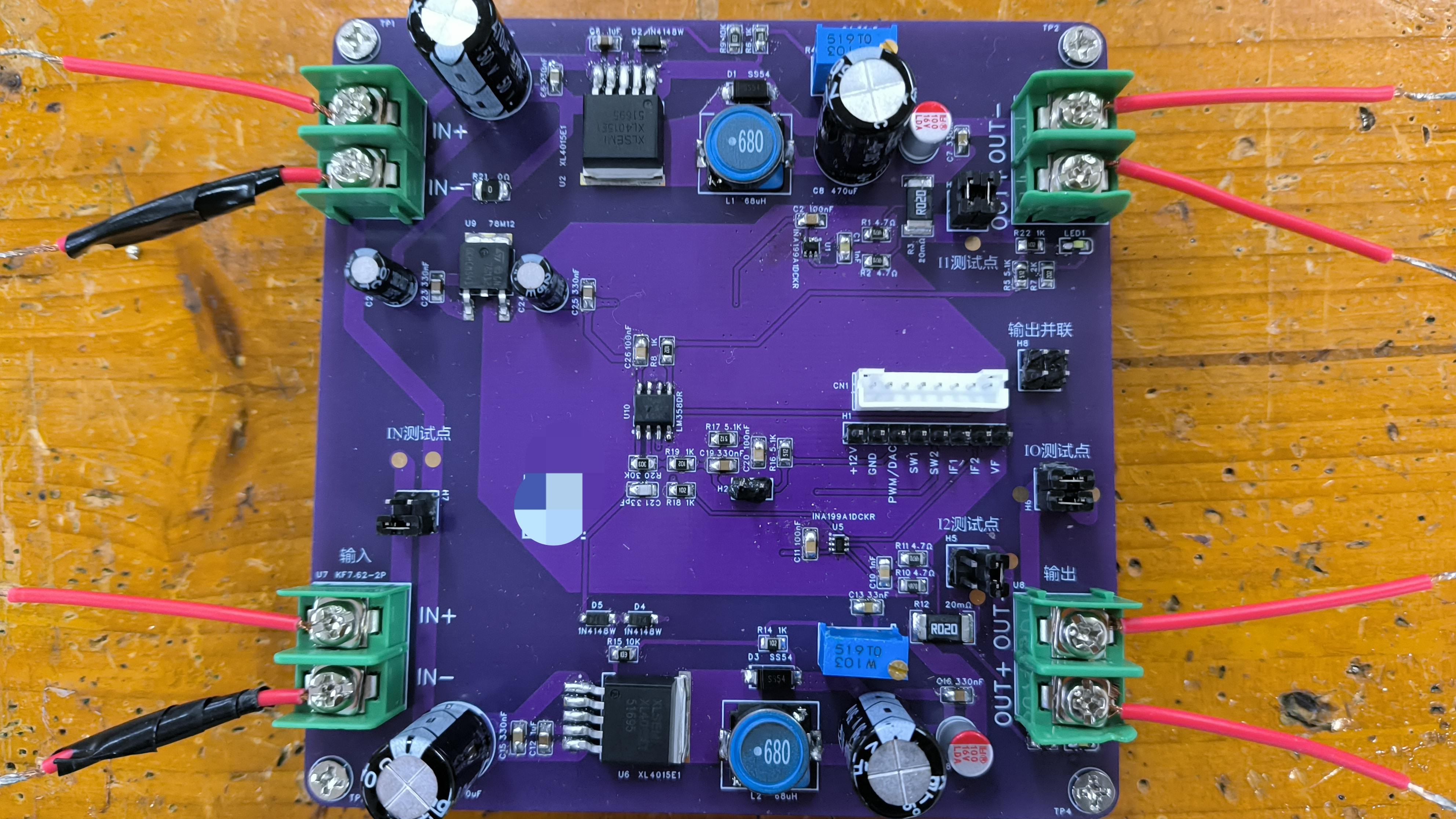
The schematic shows R3 and R12 as 20mΩ (0.02Ω) shunt resistors. If the actual current is truly 0.2A, then the voltage drop across the resistor should be:
0.2A × 0.02Ω = 0.004V (i.e., 4mV).
But your multimeter reads just 0.2mV, which suggests several possibilities:
-
Your multimeter is being interfered with by high-frequency switching noise: The XL4015 operates at around 180kHz with significant output ripple. The low-pass filter at the INA199 input (R1/R2/C1) has too high a cutoff frequency (in the MHz range), so it cannot filter out the 180kHz switching noise. When measuring tiny DC voltages superimposed with large AC ripple, a multimeter’s reading becomes unreliable.
-
Current isn’t fully flowing through the shunt resistor: Check if copper pours or traces are causing current bypassing.
Why does the gain appear to fluctuate? This is almost certainly due to switching noise coupling + poor grounding. The “output voltage” your multimeter sees is likely a signal heavily overlaid with large switching spikes. Dividing an inaccurate output by an inaccurate input results in a calculated gain wildly jumping between 2 and 200.
Suggestion: Borrow an oscilloscope and probe the output pin of the INA199—you’ll likely see a chaotic, spike-filled waveform instead of a smooth DC level.
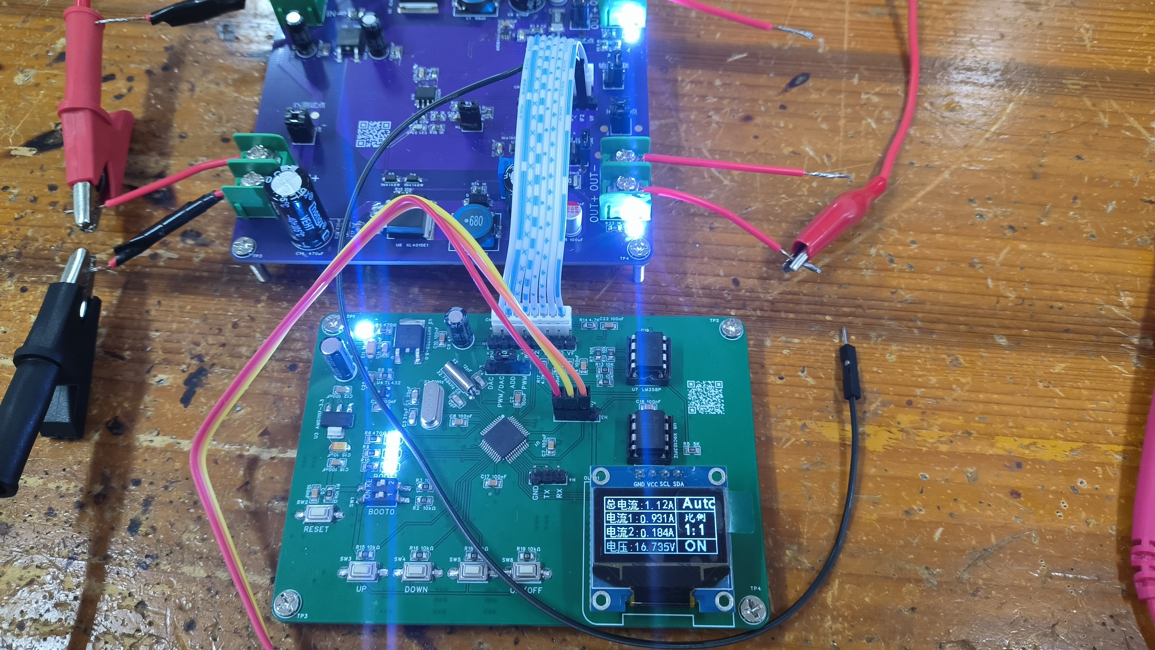
2. About OLED Display Showing Nonsensical Data and 1A Current in OFF State
-
The fatal flaw of not using Kelvin (4-wire) sensing: Your shunt resistor is 20mΩ. On a PCB with 1oz copper, even a few millimeters of trace can have several milliohms of resistance! Without Kelvin connections (i.e., separate thin traces from the inner pads of the shunt resistor directly to the INA199, avoiding high-current paths), the voltage drop across solder joints and traces gets amplified along with the signal—this explains your “current reading of 1A, which is absurd.”
-
1A “ghost current” in OFF state:
- Op-amp zero-point offset: The REF pin of the INA199 is grounded. With single-supply operation, the op-amp output cannot reach exactly 0V (usually has a lower limit of tens of millivolts). For example, if the output is stuck at 50mV, the ADC reads this, divides by a gain of 50, then divides by 20mΩ—the system falsely interprets this as a 50mA baseline current.
- Ground bounce: When you turn off one channel (or under no load), if AGND and PGND (power ground) aren’t properly managed, even a few millivolts of potential difference between grounds can be amplified by the INA199.
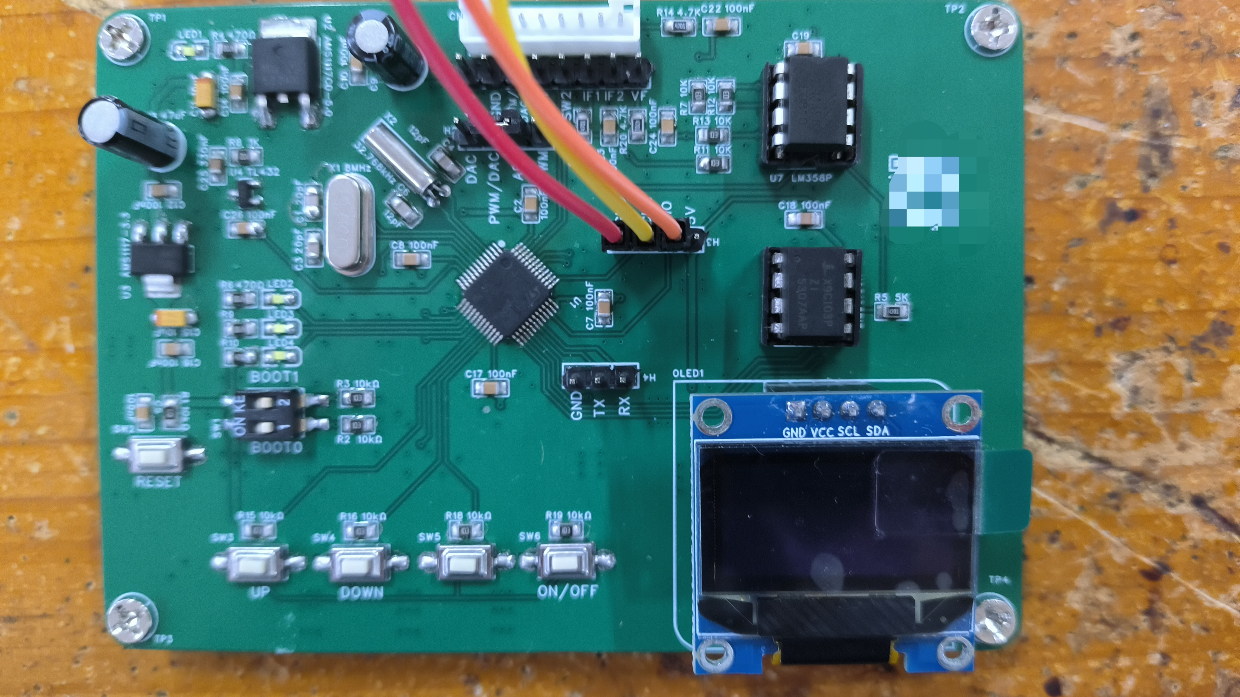
- ADC differences between STM32 and Air32: Although you changed MCUs, their internal ADC reference voltage accuracy, input impedance, and default configurations may differ slightly. The original author’s code might include “software zeroing” or calibration coefficients tailored to their board’s noise floor. After changing the MCU, the ADC reads a different baseline noise level, which the code then misinterprets as 1A.
3. Is This Design Feasible? How Should You Tune It?
Conclusion: Yes, the design is absolutely feasible—it’s actually the classic approach used in past competitions (voltage source as master, current source as slave, error amplifier for regulation). However, it is extremely sensitive to PCB layout.
Since the board is already fabricated, here’s a “controlled variable method” for hardware debugging. Don’t rush to modify software—first verify that the analog signal chain works correctly:
-
Static Injection Test (to rule out switching noise):
Power down the board. Use an external regulated power supply set to constant current mode (e.g., outputting a fixed 1A), and force this 1A directly through your shunt resistor R3.
Then power the INA199 and MCU separately with 3.3V/5V. Measure the output pin of the INA199 with a multimeter. If the output is stable at 1A \times 0.02\Omega \times 50 = 1V, then the INA199 is functional, the model is correct, and it works perfectly under pure DC conditions. This confirms the issue is 100% related to switching ripple and PCB layout.
-
Flywire “pseudo-Kelvin” modification:
Since your PCB lacks proper Kelvin connections, modify it manually. Cut the traces connecting INA199’s IN+ and IN− from the high-current copper pour, and use two very fine enameled wires to directly solder from the base metal of the 20mΩ shunt resistor to the INA199 inputs. This significantly improves accuracy in current measurement.
-
Software debouncing and calibration (for STM32):
- Increase the ADC sampling period in code.
- Implement a startup calibration: When the load is confirmed disconnected (OFF state), read the current ADC value as
Offset (zero-point offset). Then adjust all subsequent current calculations to:
Actual_Current = (ADC_Read - Offset) * coefficient.
This will eliminate the “1A ghost current” in OFF state.
-
Check ground connections (GND):
Your schematic shows AGND and GND. Where do these two grounds connect? If they’re randomly tied together, high-current return paths can interfere with the analog ground. The correct approach is single-point grounding, ideally near the negative terminal of the XL4015’s input capacitor.
Next Steps Recommendation:
If you don’t have an oscilloscope, strongly recommend performing steps 1 and 3 first—especially implementing a software-based startup noise calibration. Bro, start with the “static injection test” in step 1 to verify the INA199’s gain under pure DC. Once you complete that test, we can continue troubleshooting together.
 — Parallel Power Supply Using Switching Power Supply