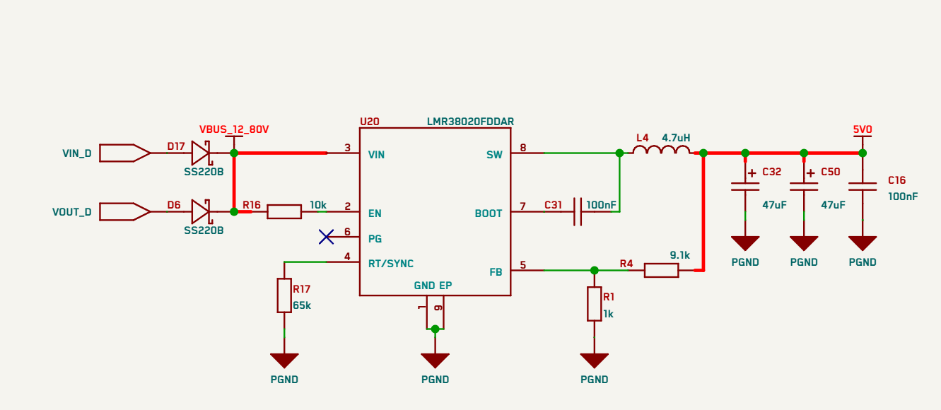
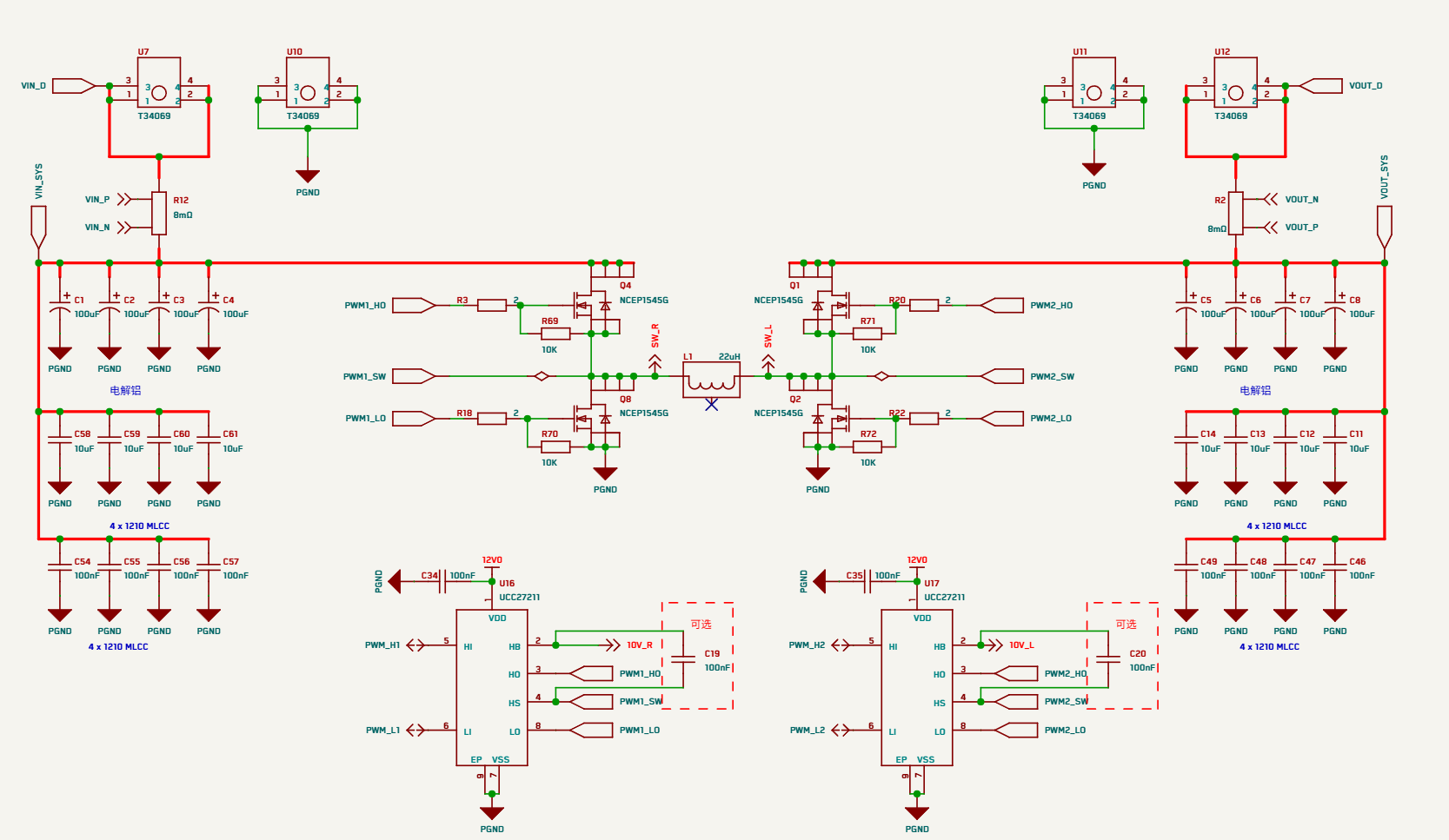
I built a bidirectional BUCK-BOOST digital power supply, with INA240A1 chips used on both sides for high-side differential sampling. The MCU and gate driver need to be powered from the system, so I implemented a dual-supply arrangement (bus-side Buck + battery-side Buck, switched with a diode OR).
Problem: No matter which side supplies power, the auxiliary supply current ultimately flows through the battery circuit’s shunt, causing very large measurement errors at low currents (<500 mA). The power calculation and coulomb counter are completely inaccurate.
You connected the power tap to the wrong spot, bro. Connect the input side of the Aux Buck to the battery/busbar terminal side of the shunt—that is, the outside of the shunt. Do not connect it on the inside of the shunt (the power circuit side). That way, the auxiliary supply current doesn’t flow through the sampling resistor at all; it just bypasses it through the port.
If the board has already been fabricated and can’t be changed, first use a PCB knife to cut the copper trace at the Aux Buck input, then fly a wire directly to the battery input terminal and try it. Small-current measurements will immediately become much cleaner.
As for the hardware, the posts above have covered what can be changed. I’ll add the software side: auxiliary current is actually calculable and measurable; it isn’t a black box:
Auxiliary current components:
MCU + peripheral quiescent current: from the datasheet plus actual measurements, basically a constant, e.g. 30–80 mA
Gate drive current: I_gate = Q_g × f_sw × N (where Q_g is the MOS gate charge, f_sw is the switching frequency, and N is the number of MOSFETs). For example, if you have 4 MOSFETs, Q_g = 50 nC, and f = 100 kHz, the drive current is 4 × 50 nC × 100k = 20 mA
Add the two together, then apply the Buck efficiency correction, and that gives the total auxiliary current
Compensation algorithm:
Determine which Buck rail is currently supplying power (compare the output voltages of the two Buck converters, or read the diode OR status)
If the battery-side Buck is supplying power: I_batt_real = I_shunt - I_aux_batt
If the bus-side Buck is supplying power (discharge mode): I_batt_real = I_shunt - P_aux/(V_batt×η), noting that P_aux must be converted using the bus-side voltage
The same applies to the Coulomb counter: subtract the corresponding equivalent charge amount during each integration period
A more robust approach: Put a small Shunt + INA199 (a few cents) in series at the auxiliary Buck output and measure the auxiliary current in real time, then subtract it dynamically in software. This is more accurate than theoretical calculation, because the drive current varies with operating conditions.
Also, a reminder: below 500 mA, your sampling signal-to-noise ratio is already poor. The INA240A1’s offset (on the order of ±25 µV) produces an error of ±2.5 mA across a 10 mΩ Shunt. After compensation at low current, don’t expect 1% accuracy. On the hardware side, you can appropriately increase the Shunt resistance.
Aux current flows battery+ → shunt → aux Buck → load → GND. It passes through the shunt directly and adds to the measured value arithmetically. Fix: relocate the Buck input to the battery terminal side of the shunt (upstream). The aux current then bypasses the measurement element entirely. Zero cost, one layout change.
Case B — bus-side Buck active, converter in discharge mode (battery → bus):
The aux power is drawn from the bus, but the bus is energized by the battery through your converter. By energy conservation, the battery supplies an additional current equal to P_aux / (V_batt · η). This component genuinely flows through the battery shunt — it is physically real, not a layout artifact. No rewiring will remove it.
For Case B you have three engineering options:
Model-based compensation in firmware. The aux load is highly predictable: MCU/static current (constant, measure once) plus gate-drive current, which is exactly Q_g · f_sw · N per switching channel. Subtract I_aux from the shunt reading each control cycle, and subtract the equivalent charge from the coulomb counter integrator.
Direct measurement. A second small-signal current monitor (INA199-class) on the aux rail gives you a live, accurate value to subtract. This handles the dynamic component of gate drive far better than a static model.
Architectural isolation. Power the MCU from an independent source and the gate drivers through isolated DC-DC converters. Eliminates the coupling entirely at the cost of BOM and board area.
I would also flag: with <500 mA of interest, verify that the INA240A1 offset voltage over your shunt value isn’t itself contributing comparable error. Compensation cannot recover information lost to noise floor.
All power take-off points are outside the high-side shunt
All of my power take-off points are outside the high-side shunt. No matter which stage is used as the input, and in the BUCK case, when the system draws power from the input, the MCU current cannot be measured at all, because the current itself does not pass through the shunt.
However, in the BOOST case, the MCU draws power from the higher-voltage side, so even if the output side appears to be externally unloaded, MCU current still flows through the shunt, which is problematic in small-current mode.
If all power take-off points were inside the high-side shunt
No matter which stage is used as the input, even when the system is unloaded and there is no output, the input side would still show the MCU current. At such low power levels, this is unfavorable for efficiency calculations.
It doesn’t care whether you’re in Buck or Boost mode; it only recognizes “which side has the higher voltage.” In Boost mode, the output-side voltage is higher, so the auxiliary power supply draws current from the output side—but the energy on the output side is boosted there from the input side through the inductor. Therefore, the input-side shunt must inevitably carry an additional current of P_aux/η.
Fix: replace the passive OR gate with active switching.
Use a P-MOS plus a small-signal NMOS to replace D6 (or replace both sides). The MCU controls the switching based on the current operating mode:
Buck mode (high voltage → low voltage): turn on the high-voltage-side MOS, turn off the low-voltage-side MOS; the auxiliary power supply draws power from the high-voltage side.
Boost mode (low voltage → high voltage): turn on the low-voltage-side MOS, turn off the high-voltage-side MOS; the auxiliary power supply draws power from the low-voltage side.
The core principle: the auxiliary power supply should always draw power from the “input side” of the power stage. The power current and auxiliary current come from the same source and flow in the same direction. The shunt measures the total current, so external load current = total current − auxiliary current. The key point is that at no load, the shunt reading is the true auxiliary current, allowing you to subtract it accurately in software instead of having it jump around on both sides due to the automatic switching of the OR gate.
The essence of this issue is that, in a bidirectional topology, the auxiliary power supply current path cannot simultaneously satisfy both “clean sampling” and “energy not passing through the shunt.” Let me sketch it out and it should become clear:
Scenario A: Power tap point is outside the shunt (your current setup)
Buck mode: The input-side voltage is higher → the OR gate selects the input → auxiliary current is drawn before the input shunt → the input shunt stays clean ✓
Boost mode: The output-side voltage is higher → the OR gate selects the output → auxiliary current is drawn before the output shunt → but the output energy comes from the input → the input shunt sees an extra current of P_aux/(V_in·η) ✗
Scenario B: Power tap point is inside the shunt
In any mode, the auxiliary current passes through the shunt → the shunt is never zero under no-load conditions ✗
So simply changing the power tap point has no solution; you must introduce either “mode awareness” or “physical isolation.”
Option 1: Mode-aware active power tapping (recommended)
As mentioned above, use MOS switches instead of diodes. The MCU controls which side the power is drawn from depending on whether the converter is currently in Buck or Boost mode, keeping the auxiliary supply connected to the input side of the power stage at all times.
Option 2: Software real-time subtraction (easiest)
Auxiliary current = MCU quiescent current (mA-level, almost constant) + gate drive current (Q_g·f_sw·N, proportional to the switching frequency). Both parts can be modeled precisely. In the control algorithm:
I_load = I_shunt - I_aux / η_buck_aux
The coulomb counter should subtract it as well. Accuracy within 1% is achievable, much faster than modifying the hardware.
Mate, you’re overthinking the hardware taps. You’ve set up a system where the MCU feeds itself from whichever side is highest. That’s a great, robust design for keeping the brain alive!
But you’re complaining that the math is “unfriendly.” Welcome to physics! In Boost mode, your MCU is literally the load. If you move the taps inside the shunts, you’ll just have the exact same headache in reverse during Buck mode.
Don’t spin a new board for this. Do a quick bench characterization: measure the actual current going into pin 3 (VIN) of your LMR38020 at different switching frequencies. Store that as a lookup table in your flash.