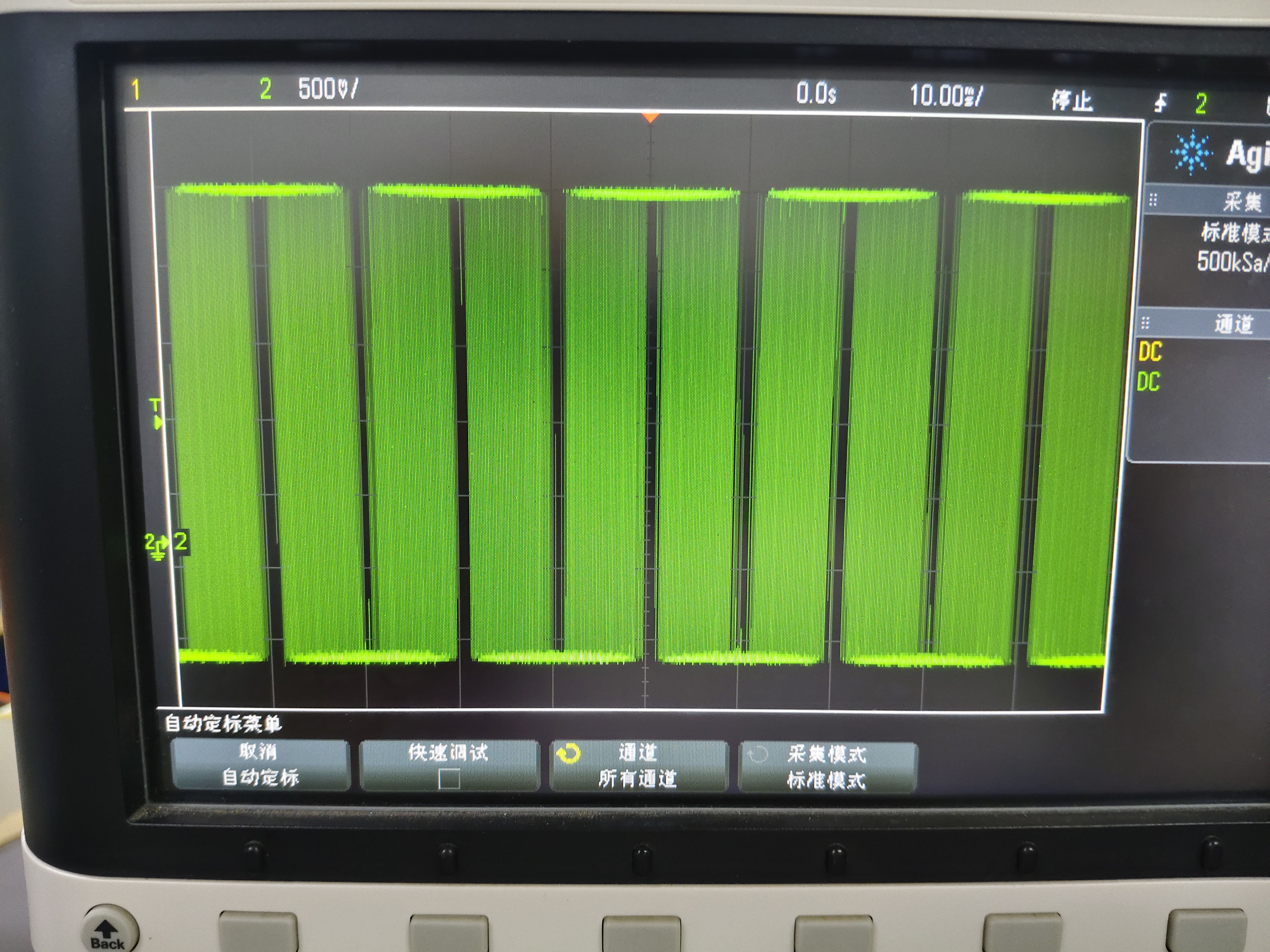
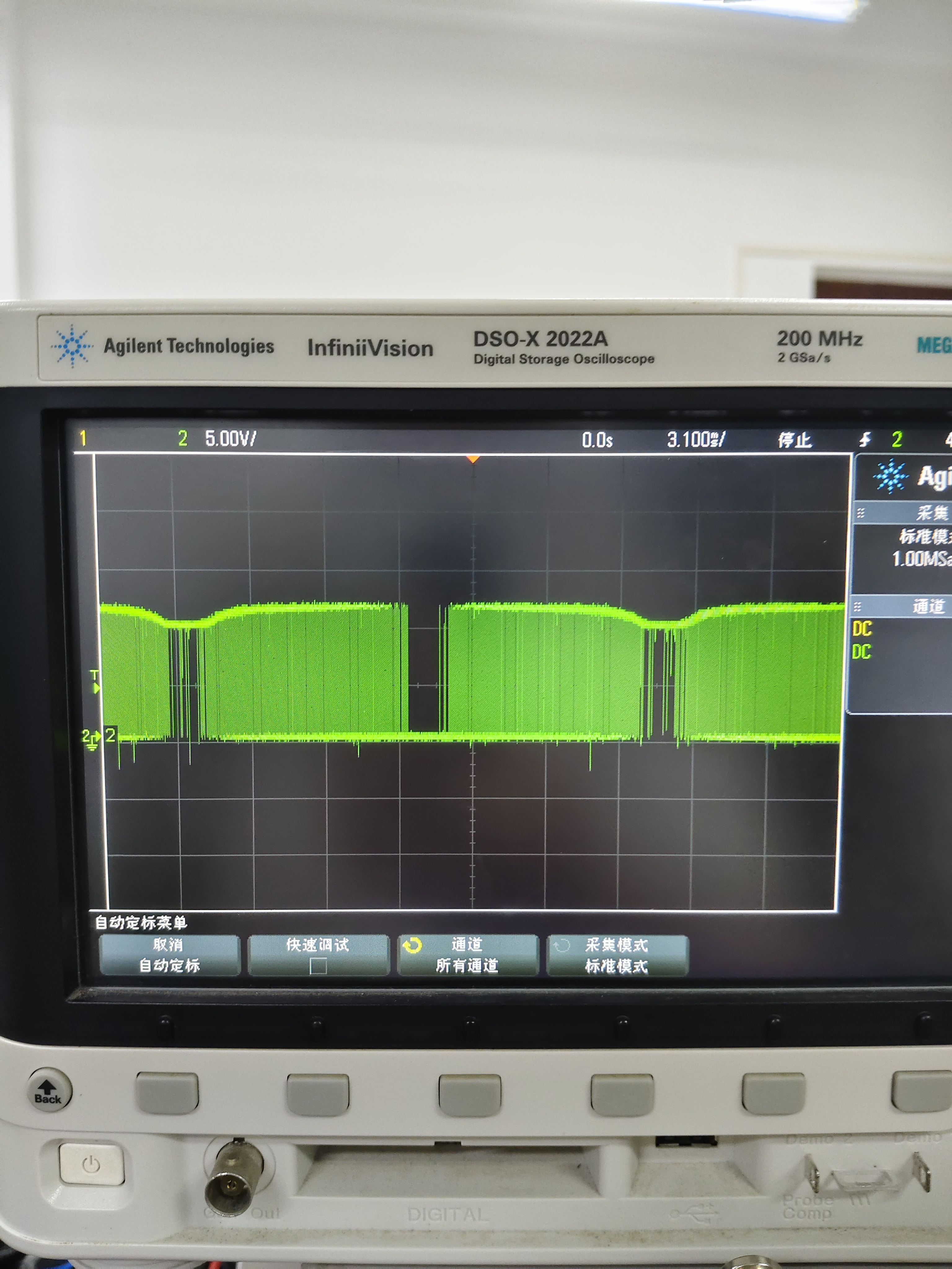
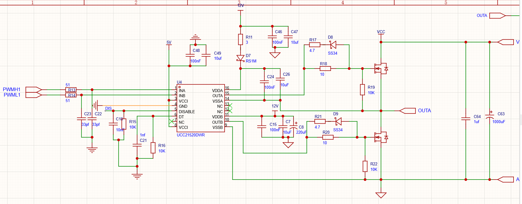
Hi everyone, I’m using the UCC21520 for a rectified-input SPWM, and the high-side waveform has a dip issue. With an input PWM wave, there’s no dip. Is the bootstrap charging time insufficient? How should I fix it? Figure 1 shows the input SP wave with a modulation ratio of 1; when I lower the modulation ratio to 0.6, there’s still a small dip. Figure 2 is the high-side output waveform. Figure 3 is the schematic—please advise.
Let me explain the mechanism thoroughly first, then tell you why you shouldn’t go down the path of “increasing the bootstrap capacitor.”
Your direction is correct: this is bootstrap starvation. When the SPWM modulation index is pulled to 1, the duty cycle in the sinusoidal peak region approaches 100%, the low-side switch hardly turns on in any carrier cycle, there is no replenishment window for the bootstrap capacitor, VDDA−VSSA keeps dropping, and once it falls below 8.2 V (the UCC21520DWR is the 8 V UVLO version), the driver shuts off and the waveform collapses in a chunk — fixed-duty PWM has a low-side window every cycle, so it is clean. The logic is completely self-consistent.
But once you finish the math, you’ll see the capacitor isn’t the bottleneck at all:
Bootstrap capacitor 10.1 µF (100 nF + 10 µF)
Driver quiescent current at most 1.8 mA; at m=1, the peak region where duty >97% lasts about 1.5 ms
Quiescent consumption 2.7 µC, plus about 1.8 µC of gate charge at the switching edges, for 4.5 µC total
4.5 µC / 10.1 µF ≈ 0.45 V droop
From 11.3 V (12 V minus the diode drop) down to the 8.2 V UVLO threshold, there is 2.6 V of margin
0.45 V versus 2.6 V — nearly an order of magnitude of headroom. The capacitance is sufficient; making it larger won’t help.
So where does the charge go? Looking at Figure 3, one part caught my eye: the bootstrap diode D7 is an RS1M with a trr of about 500 ns. Your bus is rectified high voltage; every rising edge of the SW node is instantly pulled to several hundred volts, and during reverse recovery this slow diode pulls charge backward from VDDA to 12 V — stealing once on every switching edge, stealing the whole time. This perfectly explains both of your observations at once:
The average bootstrap voltage is continuously depressed, so at m=0.6, where the maximum duty cycle is only 60–80% and starvation shouldn’t occur, you still get a small dip;
At m=1, there is no replenishment in the peak region, the stored charge is exhausted, it drops below UVLO, and the whole segment collapses.
Suggested order of action:
Measure VDDA−VSSA with a differential probe and capture it synchronously with OUTA — when the dip occurs, VDDA drops at the same time, confirming a supply problem; if VDDA is flat but OUTA dips, the problem is in the gate-drive output path or in your measurement setup itself (don’t use a long ground clip on the high side);
Replace the bootstrap diode: UF4007 (trr 75 ns), ES1J, or a SiC Schottky — it’s a one-part change; try this first;
In software, clamp the maximum duty cycle to 95–97%, guaranteeing at least one low-side replenishment window per carrier cycle; trade a few percent of output amplitude for stability — this is what inverters do;
If you need to run at 100% duty cycle, don’t use bootstrap — the UCC21520 is an isolated driver, and for the high side you really should use an isolated DC-DC; a single B0512S does the job.
This is a pitfall I’ve hit myself—the waveforms were almost identical. Fixed PWM was fine, but as soon as I switched to SPWM, a chunk was missing at the peak.
At first I also suspected the charging time wasn’t enough, so I lowered the bootstrap resistor from 10 Ω to 2.2 Ω and increased the capacitor from 0.47 µF to 2.2 µF. The notch got a little shallower, but it was still there when I pushed the modulation index to 1. Later I used a differential probe to measure VDDB with respect to VS and saw the voltage during the peak steadily dropping. Once it fell below the UVLO threshold, the drive shut off—the notch was being produced by UVLO. Only then did I understand that the low side has almost no conduction time near the peak, so the capacitor never gets a chance to charge.
While modifying it, I also hit a voltage-rating pitfall. The voltage rating of the bootstrap capacitor is chosen based on VDD, not the bus. When the high side is on, the voltage across the capacitor is still VDD; the entire capacitor’s potential is just lifted above the bus. It’s the bootstrap diode that has to be rated for the bus—it must withstand the entire bus voltage in reverse. I had these two mixed up at first, and the diode’s voltage rating wasn’t enough, so it leaked as soon as the bus voltage went high. Later I switched to a 100 V fast-recovery diode and it became stable. For a bus in the tens of volts, that’s enough; for a higher bus, leave another factor of two based on the bus. On the capacitor side, if VDD is 12 V, a 25 V rating is actually enough, but small X7R capacitors lose capacitance under DC bias, so a 50 V low-ESR part is more reassuring. After increasing the capacitor, you also need to check whether the diode can handle the charging inrush at power-up—don’t use too small a package.
In the end, I added an isolated power module for each high side, and the notch disappeared completely. If you don’t want to change the board, first limit the maximum modulation index to 0.9 and see whether the notch goes away—that’s a quick way to verify. To run at full modulation index, the bootstrap approach can’t hold up.
Bootstrap and a high modulation index are a bad marriage. The cap is a small battery that only gets charged while the low side is on. At the sine peak the high side is on for almost the whole switching period, so the low side is barely on at all. The cap drains into the driver quiescent current and the gate charge, the rail sags, UVLO trips, and you get a notch. There is nothing wrong with the SPWM signal. The bias scheme is the problem.
You can slow the sag with a bigger cap, a faster diode, and a smaller series resistor. You can shrink the notch by clamping the duty. You cannot make it vanish at m = 1 with a bootstrap, because the same cap has to be big enough to ride through the peak and small enough to recharge in the sliver of low-side time that is left. Those two conditions converge on zero.
For a one-off, a small isolated module per high-side driver is the least painful fix. Pick one with low isolation capacitance, otherwise the common-mode current will bite you. For a product, use a driver with an integrated charge pump or design a proper floating bias supply. Bootstrap is fine for a buck or a half-bridge that never runs near 100% duty. A sine-modulated bridge is not that.
Just use an isolated power supply to power VDDA and VDDB, otherwise you won’t get any of the advantages of your isolated gate driver—you might as well use a regular gate driver.